-
 Agriculture
-
 Health-Care
-
 Environment
-
 Construction-Real-Estate
-
 Tools-Hardware
-
 Home-Garden
-
 Furniture
-
 Luggage-Bags-Cases
-
 Medical-devices-Supplies
-
 Gifts-Crafts
-
 Sports-Entertainment
-
 Food-Beverage
-
 Vehicles-Transportation
-
 Power-Transmission
-
 Material-Handling
-
 Renewable-Energy
-
 Safety
-
 Testing-Instrument-Equipment
-
 Construction-Building-Machinery
-
 Pet-Supplies
-
 Personal-Care-Household-Cleaning
-
 Vehicle-Accessories-Electronics-Tools
-
 School-Office-Supplies
-
 Packaging-Printing
-
 Mother-Kids-Toys
-
 Business-Services
-
 Commercial-Equipment-Machinery
-
 Apparel-Accessories
-
 Security
-
 Shoes-Accessories
-
 Vehicle-Parts-Accessories
-
 Jewelry-Eyewear-Watches-Accessories
-
 Lights-Lighting
-
 Fabric-Textile-Raw-Material
-
 Fabrication-Services
-
 Industrial-Machinery
-
 Consumer-Electronics
-
 Electrical-Equipment-Supplies
-
 Electronic-Components-Accessories-Telecommunications
-
 Home-Appliances
-
 Beauty
-
 Chemicals
-
 Rubber-Plastics
-
 Metals-Alloys
- Masonry Materials
- Curtain Walls & Accessories
- Earthwork Products
- Fireproofing Materials
- Heat Insulation Materials
- Plastic Building Materials
- Building Boards
- Soundproofing Materials
- Timber
- Waterproofing Materials
- Balustrades & Handrails
- Bathroom & Kitchen
- Flooring & Accessories
- Tiles & Accessories
- Door, Window & Accessories
- Fireplaces & Stoves
- Floor Heating Systems & Parts
- Stairs & Stair Parts
- Ceilings
- Elevators & Escalators
- Stone
- Countertops, Vanity Tops & Table Tops
- Mosaics
- Metal Building Materials
- Multifunctional Materials
- Ladders & Scaffoldings
- Mouldings
- Corner Guards
- Decorative Films
- Formwork
- Building & Industrial Glass
- Other Construction & Real Estate
- Wallpapers/Wall panels
- HVAC System & Parts
- Outdoor Facilities
- Prefabricated Buildings
- Festive & Party Supplies
- Bathroom Products
- Household Sundries
- Rain Gear
- Garden Supplies
- Household Cleaning Tools & Accessories
- Lighters & Smoking Accessories
- Home Storage & Organization
- Household Scales
- Smart Home Improvement
- Home Textiles
- Kitchenware
- Drinkware & Accessories
- Dinnerware, Coffee & Wine
- Home Decor
- Golf
- Fitness & Body Building
- Amusement Park Facilities
- Billiards, Board Game,Coin Operated Games
- Musical Instruments
- Outdoor Affordable Luxury Sports
- Camping & Hiking
- Fishing
- Sports Safety&Rehabilitation
- Ball Sports Equipments
- Water Sports
- Winter Sports
- Luxury Travel Equipments
- Sports Shoes, Bags & Accessories
- Cycling
- Other Sports & Entertainment Products
- Artificial Grass&Sports Flooring&Sports Court Equipment
- Scooters
- Food Ingredients
- Honey & Honey Products
- Snacks
- Nuts & Kernels
- Seafood
- Plant & Animal Oil
- Beverages
- Fruit & Vegetable Products
- Frog & Escargot
- Bean Products
- Egg Products
- Dairy Products
- Seasonings & Condiments
- Canned Food
- Instant Food
- Baked Goods
- Other Food & Beverage
- Meat & Poultry
- Confectionery
- Grain Products
- Feminie Care
- Hair Care & Styling
- Body Care
- Hands & Feet Care
- Hygiene Products
- Men's Grooming
- Laundry Cleaning Supplies
- Travel Size & Gift Sets
- Room Deodorizers
- Other Personal Care Products
- Pest Control Products
- Special Household Cleaning
- Floor Cleaning
- Kitchen & Bathroom Cleaning
- Oral Care
- Bath Supplies
- Yellow Pages
- Correction Supplies
- Office Binding Supplies
- Office Cutting Supplies
- Board Erasers
- Office Adhesives & Tapes
- Education Supplies
- Pencil Cases & Bags
- Notebooks & Writing Pads
- File Folder Accessories
- Calendars
- Writing Accessories
- Commercial Office Supplies
- Pencil Sharpeners
- Pens
- Letter Pad/Paper
- Paper Envelopes
- Desk Organizers
- Pencils
- Markers & Highlighters
- Filing Products
- Art Supplies
- Easels
- Badge Holder & Accessories
- Office Paper
- Printer Supplies
- Book Covers
- Other Office & School Supplies
- Stationery Set
- Boards
- Clipboards
- Stamps
- Drafting Supplies
- Stencils
- Electronic Dictionary
- Books
- Map
- Magazines
- Calculators
- Baby & Toddler Toys
- Educational Toys
- Classic Toys
- Dress Up & Pretend Play
- Toy Vehicle
- Stuffed Animals & Plush Toys
- Outdoor Toys & Structures
- Balloons & Accessories
- Baby Food
- Children's Clothing
- Baby Supplies & Products
- Maternity Clothes
- Kids Shoes
- Baby Care
- Novelty & Gag Toys
- Dolls & Accessories
- Puzzle & Games
- Blocks & Model Building Toys
- Toddler Clothing
- Baby Clothing
- Kids' Luggage & Bags
- Arts, Crafts & DIY Toys
- Action & Toy Figures
- Baby Appliances
- Hobbies & Models
- Remote Control Toys
- Promotional Toys
- Pregnancy & Maternity
- Hygiene Products
- Kid's Textile&Bedding
- Novelty & Special Use
- Toy Weapons
- Baby Gifts
- Baby Storage & Organization
- Auto Drive Systems
- ATV/UTV Parts & Accessories
- Marine Parts & Accessories
- Other Auto Parts
- Trailer Parts & Accessories
- Auto Transmission Systems
- Train Parts & Accessories
- Universal Parts
- Railway Parts & Accessories
- Auto Brake Systems
- Aviation Parts & Accessories
- Truck Parts & Accessories
- Auto Suspension Systems
- Auto Lighting Systems
- New Energy Vehicle Parts & Accessories
- Auto Steering Systems
- Wheels, Tires & Accessories
- Bus Parts & Accessories
- Auto Performance Parts
- Cooling System
- Go-Kart & Kart Racer Parts & Accessories
- Air Conditioning Systems
- Heavy Duty Vehicle Parts & Accessories
- Auto Electrical Systems
- Auto Body Systems
- Auto Engine Systems
- Container Parts & Accessories
- Motorcycle Parts & Accessories
- Refrigeration & Heat Exchange Equipment
- Machine Tool Equipment
- Food & Beverage Machinery
- Agricultural Machinery & Equipment
- Apparel & Textile Machinery
- Chemical Machinery
- Packaging Machines
- Paper Production Machinery
- Plastic & Rubber Processing Machinery
- Industrial Robots
- Electronic Products Machinery
- Metal & Metallurgy Machinery
- Woodworking Machinery
- Home Product Manufacturing Machinery
- Machinery Accessories
- Environmental Machinery
- Machinery Service
- Electrical Equipment Manufacturing Machinery
- Industrial Compressors & Parts
- Tobacco & Cigarette Machinery
- Production Line
- Used Industrial Machinery
- Electronics Production Machinery
- Other Machinery & Industrial Equipment
- Camera, Photo & Accessories
- Portable Audio, Video & Accessories
- Television, Home Audio, Video & Accessories
- Video Games & Accessories
- Mobile Phone & Accessories
- Electronic Publications
- Earphone & Headphone & Accessories
- Speakers & Accessories
- Smart Electronics
- TV Receivers & Accessories
- Mobile Phone & Computer Repair Parts
- Chargers, Batteries & Power Supplies
- Used Electronics
- VR, AR, MR Hardware & Software
- Projectors & Presentation Equipments
- Other Consumer Electronics
- Cables & Commonly Used Accessories
- Computer Hardware & Software
- Displays, Signage and Optoelectronics
- Discrete Semiconductors
- Wireless & IoT Module and Products
- Telecommunications
- Connectors, Terminals & Accessories
- Development Boards, Electronic Modules and Kits
- Circuit Protection
- Sensors
- Isolators
- Audio Components and Products
- Integrated Circuits
- Power Supplies
- Relays
- RF, Microwave and RFID
- Electronic Accessories & Supplies
- Passive Components
- PCB & PCBA
- Air Quality Appliances
- Home Appliance Parts
- Heating & Cooling Appliances
- Small Kitchen Appliances
- Laundry Appliances
- Water Heaters
- Water Treatment Appliances
- Refrigerators & Freezers
- Personal Care & Beauty Appliances
- Major Kitchen Appliances
- Cleaning Appliances
- Second-hand Appliances
- Smart Home Appliances
- Other Home Appliances
- Energy Chemicals
- Inorganic Chemicals
- Basic Organic Chemicals
- Agrochemicals
- Admixture & Additives
- Catalysts & Chemical Auxiliary Agents
- Pigments & Dyestuff
- Coating & Paint
- Daily Chemicals
- Polymer
- Organic Intermediate
- Adhesives & Sealants
- Chemical Waste
- Biological Chemical Products
- Surface Treatment Chemicals
- Painting & Coating
- Chemical Reagents
- Flavor & Fragrance
- Non-Explosive Demolition Agents
- Other Chemicals
- Custom Chemical Services
Electronic Accessories & Supplies

Next Generation Television Studio Lighting Boards With Integrated Smart Control And Monitoring
In the dynamic world of television production, lighting is not merely an artistic endeavor but a critical technical foundation that shapes the visual narrative and emotional impact of every broadcast. For decades, lighting control has relied on complex consoles operated by skilled technicians, often involving manual adjustments and reactive problem-solving. However, the industry is undergoing a profound transformation, driven by the advent of the Next Generation Television Studio Lighting Boards with Integrated Smart Control and Monitoring. These systems represent a paradigm shift, merging advanced hardware with intelligent software to create a unified, automated, and data-driven lighting ecosystem. This evolution promises to enhance creative flexibility, streamline operations, and ensure unprecedented reliability, fundamentally changing how studios approach illumination for live events, news broadcasts, and scripted content.
Architectural Integration and Centralized Command
The core of next-generation lighting boards lies in their fully integrated architecture. Unlike traditional setups where lighting control, power management, and diagnostic tools often function as separate entities, these new consoles combine all elements into a single, cohesive platform. The lighting board itself evolves from a mere controller into a central command hub. It seamlessly interfaces with LED fixtures, conventional luminaires, motorized rigging, and even environmental sensors through standardized protocols like DMX, Art-Net, sACN, and emerging IoT frameworks.
This integration allows for holistic scene management. A director of photography or lighting designer can now manipulate not just intensity and color, but also focus, beam shaping, and fixture positioning from one interface. The system can store and recall complex lighting states for different scenes or shows with a single command, dramatically reducing setup times between productions. Furthermore, this centralized approach enables the lighting system to communicate bidirectionally with other studio systems, such as camera robotics and audio consoles, allowing for synchronized cues where lighting changes are perfectly timed with camera moves or audio effects, creating a more immersive production.
Intelligent Automation and Adaptive Control
Smart control is the defining feature that elevates these boards beyond their predecessors. Leveraging artificial intelligence and machine learning algorithms, the systems can automate routine and complex tasks. For instance, they can automatically adjust fixture intensities and color temperatures based on real-time feedback from cameras to maintain consistent exposure and white balance, even as subjects move within the studio. This is particularly valuable for live news or talk shows where lighting conditions must remain flawless without constant manual tweaking.
Beyond reactivity, these systems offer predictive and adaptive capabilities. They can learn from past shows to suggest optimal lighting plots for similar setups. During a production, smart monitoring can track the health and performance of each fixture, predicting potential failures like LED degradation or color shift before they affect the broadcast. The system can then automatically re-route control signals or adjust neighboring fixtures to compensate, ensuring the show goes on without a visible hitch. This level of automation empowers creative teams to focus more on artistic expression and less on technical minutiae.
Comprehensive Real-Time Monitoring and Analytics
Integrated monitoring transforms the lighting board into a powerful diagnostic and management tool. Every connected fixture becomes a node in a network, continuously reporting a wealth of data back to the console. This includes not just basic status (on/off), but detailed metrics such as real-time power consumption, internal temperature, operating hours, colorimetric data, and signal integrity. This information is displayed on intuitive dashboards, often with graphical representations of the rig, where a technician can see the health of the entire system at a glance.
The power of this monitoring lies in its actionable analytics. The system can generate reports on energy usage per show or fixture, aiding in sustainability efforts and cost management. It can alert crews to anomalies, such as a fixture drawing too much current or a DMX line experiencing interference, pinpointing the exact location of the issue. This proactive maintenance capability minimizes downtime and reduces the need for time-consuming physical checks of often hard-to-reach fixtures. In essence, the lighting board becomes the central nervous system of the studio's visual infrastructure, providing unparalleled visibility and control.
Enhanced User Experience and Creative Empowerment
The user interface of next-generation boards is designed for both power and accessibility. Touchscreen displays with customizable layouts allow operators to create workspaces tailored to their specific role—whether they are a programmer building complex cues or an operator running a live show. Gesture controls, voice commands, and even tablet-based wireless remotes offer flexible interaction models. The software often includes visual scripting tools or node-based programming environments, making it easier to design sophisticated, conditional lighting sequences that would be cumbersome to program manually.
This technological leap profoundly empowers the creative process. Lighting designers can experiment with virtual pre-visualization, building and testing looks in a 3D software model of the studio that is directly linked to the physical board. Once satisfied, they can transfer the entire design to the real rig with high fidelity. The reduction in technical barriers allows for more ambitious lighting designs, fostering innovation in visual storytelling. Ultimately, these systems democratize advanced lighting techniques, making them more accessible to productions of all scales and budgets.

Professional Grade Television Lighting PCBs With Enhanced Thermal Management And Longevity Features
In the rapidly evolving world of television production and high-end consumer displays, the demand for superior image quality, reliability, and energy efficiency has never been higher. At the heart of modern LED-backlit and direct-lit televisions lies a critical, yet often overlooked component: the lighting printed circuit board (PCB). While standard PCBs perform adequately for everyday electronics, professional-grade television applications require a specialized breed of lighting PCBs engineered to withstand intense thermal loads and ensure exceptional longevity. This article delves into the sophisticated world of Professional Grade Television Lighting PCBs with Enhanced Thermal Management and Longevity Features, exploring the advanced technologies that power the brilliant, consistent, and durable visuals we experience on premium screens today. Understanding these innovations provides insight into how manufacturers achieve stunning picture quality that lasts, making it a compelling topic for industry professionals, tech enthusiasts, and discerning consumers alike.
Advanced Thermal Management Systems
The primary challenge in high-brightness television LED arrays is heat dissipation. Unlike conventional PCBs, professional-grade lighting PCBs are designed with a multi-faceted thermal management strategy. This begins with the substrate material itself. While standard FR-4 materials are common, professional PCBs often utilize metal-core PCBs (MCPCBs), typically with an aluminum or copper base. These materials possess exceptionally high thermal conductivity, allowing heat generated by the high-power LED chips to be rapidly transferred away from the sensitive semiconductor junctions.
Beyond the core material, the design incorporates sophisticated thermal vias and extensive copper pours in the internal layers. Thermal vias are plated-through holes that act as heat pipes, channeling thermal energy from the surface-mounted LEDs down into the underlying metal core or dedicated heat sink layers. This intricate network ensures there are no localized hot spots, which are a leading cause of premature LED failure and color shift. Furthermore, the physical layout of the PCB is meticulously planned to maximize surface area for heat dissipation, often integrating the PCB directly into the television's structural heat sink or chassis, creating a unified thermal solution that operates with high efficiency even under prolonged peak brightness.
Enhanced Longevity and Reliability Features
Longevity in professional television lighting is non-negotiable, as these systems are expected to perform flawlessly for tens of thousands of hours. Enhanced PCBs achieve this through material selection and protective coatings. The copper traces are frequently thicker and made with high-purity, oxygen-free copper to reduce electrical resistance and minimize heat generation due to current flow. This also enhances the current-carrying capacity, preventing trace delamination or burnout under high load.
A critical longevity feature is the application of specialized conformal coatings. These coatings, such as silicone or acrylic-based layers, are applied over the assembled PCB. They provide a robust barrier against environmental contaminants like dust, moisture, and corrosive gases that can lead to electrochemical migration and short circuits. Additionally, the soldering process uses high-temperature, lead-free solder alloys with superior fatigue resistance to withstand the constant thermal cycling—heating when on and cooling when off—that television boards endure daily. The combination of robust materials and protective measures significantly extends the mean time between failures (MTBF), ensuring consistent color performance and light output over the display's entire lifespan.
Precision Electrical Performance and Signal Integrity
For professional-grade televisions, especially those used in color-critical applications like broadcast studios or medical imaging, consistent and precise light output is paramount. The lighting PCB must deliver stable power to each LED or mini-LED zone. This is achieved through meticulous PCB design that minimizes parasitic inductance and capacitance. Dedicated power and ground planes are used to provide a low-impedance path for current, reducing voltage drops and ensuring every LED in an array receives an identical voltage, which is crucial for uniform brightness.
In advanced local dimming systems, where hundreds or thousands of zones are individually controlled, the PCB's role becomes even more complex. The board must accommodate dense networks of control signal traces without crosstalk or interference. High-quality dielectric materials with stable electrical properties across a wide temperature range are essential to maintain signal integrity. Impedance control for high-speed dimming signals is carefully managed during the PCB fabrication process to prevent timing errors and ensure the rapid, accurate modulation of light required for deep blacks and high dynamic range (HDR) content.
Robust Mechanical Design and Manufacturing Standards
The mechanical robustness of a lighting PCB directly impacts its survival in the final product. Professional-grade PCBs are designed to resist warping from thermal stress and physical vibration. This involves using materials with matched coefficients of thermal expansion (CTE) where possible. For instance, the CTE of the solder mask, copper layers, and substrate are engineered to expand and contract at similar rates during temperature fluctuations, preventing stress fractures in solder joints.
Manufacturing these boards adheres to stringent standards, often surpassing IPC Class 2 or 3 requirements for electronic assemblies. This includes automated optical inspection (AOI) for soldering defects, X-ray inspection for hidden issues like voiding in thermal vias, and rigorous electrical testing. The components themselves, from the LED packages to the smallest decoupling capacitor, are sourced for high-temperature operation and long-term stability. This holistic approach to mechanical and manufacturing integrity ensures that the lighting PCB is not the weak link in a premium television, capable of enduring the rigors of shipping, installation, and years of continuous operation.

High Precision Lighting Control PCB Solutions Tailored For Modern TV Studio Environments
In the dynamic world of modern television production, where every frame is scrutinized in ultra-high definition and live broadcasts demand flawless execution, lighting is far more than mere illumination. It is a critical storytelling tool, shaping mood, directing viewer attention, and ensuring color accuracy. The backbone of this sophisticated lighting artistry is no longer just the fixture itself, but the intelligent, unseen technology that commands it: the High Precision Lighting Control PCB (Printed Circuit Board). This article delves into the specialized world of PCB solutions engineered explicitly for the rigorous demands of contemporary TV studios, exploring how these compact yet powerful boards are revolutionizing broadcast environments by offering unprecedented control, reliability, and integration.
Unparalleled Control Accuracy and Signal Integrity
The primary mandate for any TV studio lighting system is precise, repeatable control. High Precision Lighting Control PCBs are designed to meet this need at the most fundamental electronic level. They utilize advanced microcontrollers and digital signal processors (DSPs) capable of executing complex dimming curves—such as logarithmic or square law—with exceptional fidelity. This ensures that a lighting director's command for a 10% intensity increase translates to an exact, smooth, and flicker-free adjustment in the fixture, crucial for maintaining consistent exposure during slow fades or dramatic cues.
Furthermore, signal integrity is paramount in the electrically noisy environment of a studio packed with cameras, monitors, and power cables. These specialized PCBs incorporate robust design principles: multi-layer boards with dedicated ground planes, high-quality filtering components, and shielded communication interfaces. This architecture minimizes electromagnetic interference (EMI) and crosstalk, ensuring that control signals for hundreds of channels remain clean and uncompromised. Whether receiving DMX512, Art-Net, sACN, or proprietary digital protocols, the PCB acts as a reliable interpreter, guaranteeing that the artistic intent is perfectly executed by the LED arrays or conventional dimmers.
Thermal Management and Long-Term Reliability
TV studios operate for extended periods, often under hot lighting loads. The control PCBs within lighting fixtures and dimmer racks are subjected to significant thermal stress. High Precision solutions address this through meticulous thermal design. This involves the strategic placement of heat-generating components like power MOSFETs or drivers, the use of thermally conductive substrates (e.g., metal-core PCBs or ceramics for high-power applications), and the integration of thermal pads and vias to dissipate heat efficiently to heatsinks.
This focus on thermal management is directly linked to system longevity and stability. By maintaining optimal operating temperatures, these PCBs prevent the premature aging of components, particularly electrolytic capacitors and semiconductors. Enhanced reliability means reduced downtime—a critical factor during a live news broadcast or a prime-time show. Manufacturers of these solutions often subject their PCBs to rigorous environmental stress testing, ensuring they can withstand the thermal cycling and sustained operation endemic to 24/7 broadcast facilities.
Seamless Integration and Networked Intelligence
Modern TV studios are ecosystems of interconnected devices. A lighting control PCB is no longer an isolated component but a networked node. Advanced solutions feature embedded networking capabilities, such as Ethernet ports or wireless modules, allowing them to be part of a larger IoT-style infrastructure. They can receive timecode for synchronization with video playback, respond to triggers from automation systems for pre-programmed scene changes, and report their status back to a central monitoring dashboard.
This intelligence extends to diagnostics and configurability. On-board sensors can monitor output current, voltage, and temperature, enabling predictive maintenance by alerting technicians to potential issues before they cause a failure. Furthermore, many high-precision PCBs are firmware-upgradable via the network. This allows studios to add new features, improve performance, or adapt to new lighting protocols without physically replacing hardware, offering a future-proof investment and unparalleled flexibility in a rapidly evolving technological landscape.
Miniaturization and Customization for Diverse Form Factors
The trend in studio lighting, especially with LED technology, is toward smaller, more versatile fixtures. High Precision Control PCBs have kept pace through significant miniaturization. Using surface-mount technology (SMT), high-density interconnect (HDI) layouts, and compact component packages, engineers pack powerful control logic into remarkably small footprints. This enables the design of sleek, lightweight fixtures that can be mounted in tight spaces on set or within intricate lighting grids.
Perhaps most importantly, these PCB solutions are often tailored—or readily customizable—for specific studio applications. A PCB for a high-power LED Fresnel will have a different power stage design than one for a low-voltage LED tape or a legacy tungsten dimmer module. Leading providers work closely with lighting manufacturers to develop application-specific solutions, optimizing the circuit for the exact voltage, current, control protocol, and form factor required. This bespoke approach ensures that each lighting instrument performs at its peak, contributing to a cohesive and precisely controllable studio lighting rig.
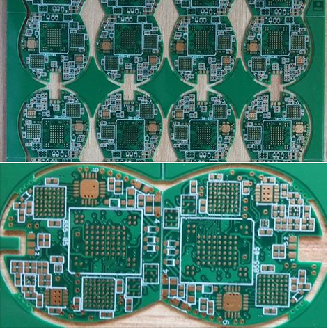
Robust Ceramic Board Construction Ensuring Longevity And Performance In Microwave RF PCBs
In the rapidly advancing world of high-frequency electronics, Microwave and Radio Frequency (RF) Printed Circuit Boards (PCBs) are the unsung heroes enabling technologies from satellite communications to 5G networks and advanced radar systems. At the heart of these critical applications lies a fundamental challenge: how to maintain signal integrity, manage immense thermal loads, and ensure unwavering reliability under demanding operational conditions. The answer increasingly points toward one pivotal innovation—robust ceramic board construction. Unlike traditional organic substrates like FR-4, ceramic materials such as alumina (Al2O3), aluminum nitride (AlN), and beryllia (BeO) offer a unique combination of properties that are indispensable for high-performance microwave RF circuits. This article delves into how the inherent robustness of ceramic substrates is not merely an enhancement but a foundational requirement for ensuring both the longevity and peak performance of modern microwave RF PCBs, exploring the material science and engineering principles that make them the substrate of choice for cutting-edge applications.
Superior Electrical Performance at High Frequencies
The primary driver for adopting ceramic substrates in microwave RF PCBs is their exceptional electrical performance. At microwave frequencies, signal loss and dispersion become critical concerns. Organic substrates often exhibit higher dielectric loss tangents, meaning they absorb more electromagnetic energy, converting it into heat and degrading signal strength. Ceramic materials, particularly high-purity alumina or specialized compositions, feature exceptionally low loss tangents. This characteristic ensures minimal signal attenuation as high-frequency waves propagate across the circuit, preserving the integrity of sensitive RF signals.
Furthermore, the dielectric constant of ceramics is highly stable and predictable over a wide frequency and temperature range. This stability is paramount for designing precise impedance-controlled transmission lines, such as microstrips and coplanar waveguides, which are the backbone of RF circuits. A stable dielectric constant prevents impedance mismatches that can lead to signal reflections, standing waves, and ultimately, reduced system efficiency. The inherent homogeneity of ceramic boards also eliminates the variations often found in laminated organics, providing consistent electrical properties across the entire board and from batch to batch, which is crucial for mass production of reliable RF components.
Exceptional Thermal Management Capabilities
Thermal management is arguably the most critical factor influencing the longevity and reliability of any electronic system, and it is especially acute in high-power microwave RF applications. Power amplifiers, oscillators, and other active components generate significant heat, which, if not efficiently dissipated, leads to performance drift, accelerated aging, and catastrophic failure. Ceramic substrates excel in this domain due to their high thermal conductivity. For instance, aluminum nitride (AlN) boasts a thermal conductivity several times greater than alumina and orders of magnitude higher than standard FR-4.
This superior thermal conductivity allows heat to be rapidly spread away from hot spots and transferred to heatsinks or the environment. By maintaining lower operating temperatures, ceramic boards ensure that semiconductor devices operate within their optimal thermal windows, preserving their electrical characteristics and dramatically extending their operational lifespan. Additionally, ceramics have a Coefficient of Thermal Expansion (CTE) that can be closely matched to critical components like semiconductor dies and packages. This CTE matching minimizes mechanical stress during thermal cycling—a common occurrence in operational environments—preventing solder joint fatigue, delamination, and cracks that plague mismatched material systems.
Mechanical Robustness and Environmental Stability
The longevity of a PCB is determined not just by its electrical performance under ideal conditions, but by its ability to withstand physical and environmental challenges over years of service. Ceramic boards are inherently robust. They exhibit high mechanical strength, rigidity, and hardness, making them resistant to bending, flexing, and physical deformation that can damage delicate circuit traces. This structural integrity is vital for applications subject to vibration or shock, such as in aerospace, automotive radar, or portable military equipment.
Beyond physical strength, ceramics offer outstanding environmental stability. They are chemically inert, non-porous, and impervious to moisture absorption. Unlike organic substrates that can absorb ambient humidity—leading to changes in dielectric properties and potential leakage currents—ceramics remain dimensionally and electrically stable in humid conditions. They are also resistant to most solvents and corrosive agents, and can operate reliably across an extremely wide temperature range, from cryogenic levels to several hundred degrees Celsius. This combination of traits ensures that microwave RF PCBs built on ceramic foundations can endure harsh environments, from the vacuum of space to the under-the-hood heat of an automobile, without degradation.
Advanced Manufacturing and Integration Potential
The construction of robust ceramic boards leverages advanced manufacturing techniques that further enhance performance and integration. Processes like Low Temperature Co-fired Ceramic (LTCC) and High Temperature Co-fired Ceramic (HTCC) allow for the creation of complex, multi-layer three-dimensional structures within a single, monolithic substrate. These technologies enable the embedding of passive components like resistors, inductors, and capacitors, as well as the creation of sealed cavities and intricate via structures for grounding and shielding.
This level of integration minimizes parasitic effects and interconnect lengths, which is critical for maintaining performance at microwave frequencies. It also leads to a significant reduction in the overall size and weight of the RF module—a key advantage for modern compact devices. The precision achievable with ceramic processing, including thick-film and thin-film metallization, allows for the creation of extremely fine features and high-density interconnects necessary for today's complex RF systems. The result is a highly reliable, integrated subsystem where the robustness of the ceramic material is complemented by a manufacturing process designed for maximum performance and miniaturization.
REPORT


