-
 Agriculture
-
 Health-Care
-
 Environment
-
 Construction-Real-Estate
-
 Tools-Hardware
-
 Home-Garden
-
 Furniture
-
 Luggage-Bags-Cases
-
 Medical-devices-Supplies
-
 Gifts-Crafts
-
 Sports-Entertainment
-
 Food-Beverage
-
 Vehicles-Transportation
-
 Power-Transmission
-
 Material-Handling
-
 Renewable-Energy
-
 Safety
-
 Testing-Instrument-Equipment
-
 Construction-Building-Machinery
-
 Pet-Supplies
-
 Personal-Care-Household-Cleaning
-
 Vehicle-Accessories-Electronics-Tools
-
 School-Office-Supplies
-
 Packaging-Printing
-
 Mother-Kids-Toys
-
 Business-Services
-
 Commercial-Equipment-Machinery
-
 Apparel-Accessories
-
 Security
-
 Shoes-Accessories
-
 Vehicle-Parts-Accessories
-
 Jewelry-Eyewear-Watches-Accessories
-
 Lights-Lighting
-
 Fabric-Textile-Raw-Material
-
 Fabrication-Services
-
 Industrial-Machinery
-
 Consumer-Electronics
-
 Electrical-Equipment-Supplies
-
 Electronic-Components-Accessories-Telecommunications
-
 Home-Appliances
-
 Beauty
-
 Chemicals
-
 Rubber-Plastics
-
 Metals-Alloys
- Masonry Materials
- Curtain Walls & Accessories
- Earthwork Products
- Fireproofing Materials
- Heat Insulation Materials
- Plastic Building Materials
- Building Boards
- Soundproofing Materials
- Timber
- Waterproofing Materials
- Balustrades & Handrails
- Bathroom & Kitchen
- Flooring & Accessories
- Tiles & Accessories
- Door, Window & Accessories
- Fireplaces & Stoves
- Floor Heating Systems & Parts
- Stairs & Stair Parts
- Ceilings
- Elevators & Escalators
- Stone
- Countertops, Vanity Tops & Table Tops
- Mosaics
- Metal Building Materials
- Multifunctional Materials
- Ladders & Scaffoldings
- Mouldings
- Corner Guards
- Decorative Films
- Formwork
- Building & Industrial Glass
- Other Construction & Real Estate
- Wallpapers/Wall panels
- HVAC System & Parts
- Outdoor Facilities
- Prefabricated Buildings
- Festive & Party Supplies
- Bathroom Products
- Household Sundries
- Rain Gear
- Garden Supplies
- Household Cleaning Tools & Accessories
- Lighters & Smoking Accessories
- Home Storage & Organization
- Household Scales
- Smart Home Improvement
- Home Textiles
- Kitchenware
- Drinkware & Accessories
- Dinnerware, Coffee & Wine
- Home Decor
- Golf
- Fitness & Body Building
- Amusement Park Facilities
- Billiards, Board Game,Coin Operated Games
- Musical Instruments
- Outdoor Affordable Luxury Sports
- Camping & Hiking
- Fishing
- Sports Safety&Rehabilitation
- Ball Sports Equipments
- Water Sports
- Winter Sports
- Luxury Travel Equipments
- Sports Shoes, Bags & Accessories
- Cycling
- Other Sports & Entertainment Products
- Artificial Grass&Sports Flooring&Sports Court Equipment
- Scooters
- Food Ingredients
- Honey & Honey Products
- Snacks
- Nuts & Kernels
- Seafood
- Plant & Animal Oil
- Beverages
- Fruit & Vegetable Products
- Frog & Escargot
- Bean Products
- Egg Products
- Dairy Products
- Seasonings & Condiments
- Canned Food
- Instant Food
- Baked Goods
- Other Food & Beverage
- Meat & Poultry
- Confectionery
- Grain Products
- Feminie Care
- Hair Care & Styling
- Body Care
- Hands & Feet Care
- Hygiene Products
- Men's Grooming
- Laundry Cleaning Supplies
- Travel Size & Gift Sets
- Room Deodorizers
- Other Personal Care Products
- Pest Control Products
- Special Household Cleaning
- Floor Cleaning
- Kitchen & Bathroom Cleaning
- Oral Care
- Bath Supplies
- Yellow Pages
- Correction Supplies
- Office Binding Supplies
- Office Cutting Supplies
- Board Erasers
- Office Adhesives & Tapes
- Education Supplies
- Pencil Cases & Bags
- Notebooks & Writing Pads
- File Folder Accessories
- Calendars
- Writing Accessories
- Commercial Office Supplies
- Pencil Sharpeners
- Pens
- Letter Pad/Paper
- Paper Envelopes
- Desk Organizers
- Pencils
- Markers & Highlighters
- Filing Products
- Art Supplies
- Easels
- Badge Holder & Accessories
- Office Paper
- Printer Supplies
- Book Covers
- Other Office & School Supplies
- Stationery Set
- Boards
- Clipboards
- Stamps
- Drafting Supplies
- Stencils
- Electronic Dictionary
- Books
- Map
- Magazines
- Calculators
- Baby & Toddler Toys
- Educational Toys
- Classic Toys
- Dress Up & Pretend Play
- Toy Vehicle
- Stuffed Animals & Plush Toys
- Outdoor Toys & Structures
- Balloons & Accessories
- Baby Food
- Children's Clothing
- Baby Supplies & Products
- Maternity Clothes
- Kids Shoes
- Baby Care
- Novelty & Gag Toys
- Dolls & Accessories
- Puzzle & Games
- Blocks & Model Building Toys
- Toddler Clothing
- Baby Clothing
- Kids' Luggage & Bags
- Arts, Crafts & DIY Toys
- Action & Toy Figures
- Baby Appliances
- Hobbies & Models
- Remote Control Toys
- Promotional Toys
- Pregnancy & Maternity
- Hygiene Products
- Kid's Textile&Bedding
- Novelty & Special Use
- Toy Weapons
- Baby Gifts
- Baby Storage & Organization
- Auto Drive Systems
- ATV/UTV Parts & Accessories
- Marine Parts & Accessories
- Other Auto Parts
- Trailer Parts & Accessories
- Auto Transmission Systems
- Train Parts & Accessories
- Universal Parts
- Railway Parts & Accessories
- Auto Brake Systems
- Aviation Parts & Accessories
- Truck Parts & Accessories
- Auto Suspension Systems
- Auto Lighting Systems
- New Energy Vehicle Parts & Accessories
- Auto Steering Systems
- Wheels, Tires & Accessories
- Bus Parts & Accessories
- Auto Performance Parts
- Cooling System
- Go-Kart & Kart Racer Parts & Accessories
- Air Conditioning Systems
- Heavy Duty Vehicle Parts & Accessories
- Auto Electrical Systems
- Auto Body Systems
- Auto Engine Systems
- Container Parts & Accessories
- Motorcycle Parts & Accessories
- Refrigeration & Heat Exchange Equipment
- Machine Tool Equipment
- Food & Beverage Machinery
- Agricultural Machinery & Equipment
- Apparel & Textile Machinery
- Chemical Machinery
- Packaging Machines
- Paper Production Machinery
- Plastic & Rubber Processing Machinery
- Industrial Robots
- Electronic Products Machinery
- Metal & Metallurgy Machinery
- Woodworking Machinery
- Home Product Manufacturing Machinery
- Machinery Accessories
- Environmental Machinery
- Machinery Service
- Electrical Equipment Manufacturing Machinery
- Industrial Compressors & Parts
- Tobacco & Cigarette Machinery
- Production Line
- Used Industrial Machinery
- Electronics Production Machinery
- Other Machinery & Industrial Equipment
- Camera, Photo & Accessories
- Portable Audio, Video & Accessories
- Television, Home Audio, Video & Accessories
- Video Games & Accessories
- Mobile Phone & Accessories
- Electronic Publications
- Earphone & Headphone & Accessories
- Speakers & Accessories
- Smart Electronics
- TV Receivers & Accessories
- Mobile Phone & Computer Repair Parts
- Chargers, Batteries & Power Supplies
- Used Electronics
- VR, AR, MR Hardware & Software
- Projectors & Presentation Equipments
- Other Consumer Electronics
- Cables & Commonly Used Accessories
- Computer Hardware & Software
- Displays, Signage and Optoelectronics
- Discrete Semiconductors
- Wireless & IoT Module and Products
- Telecommunications
- Connectors, Terminals & Accessories
- Development Boards, Electronic Modules and Kits
- Circuit Protection
- Sensors
- Isolators
- Audio Components and Products
- Integrated Circuits
- Power Supplies
- Relays
- RF, Microwave and RFID
- Electronic Accessories & Supplies
- Passive Components
- PCB & PCBA
- Air Quality Appliances
- Home Appliance Parts
- Heating & Cooling Appliances
- Small Kitchen Appliances
- Laundry Appliances
- Water Heaters
- Water Treatment Appliances
- Refrigerators & Freezers
- Personal Care & Beauty Appliances
- Major Kitchen Appliances
- Cleaning Appliances
- Second-hand Appliances
- Smart Home Appliances
- Other Home Appliances
- Energy Chemicals
- Inorganic Chemicals
- Basic Organic Chemicals
- Agrochemicals
- Admixture & Additives
- Catalysts & Chemical Auxiliary Agents
- Pigments & Dyestuff
- Coating & Paint
- Daily Chemicals
- Polymer
- Organic Intermediate
- Adhesives & Sealants
- Chemical Waste
- Biological Chemical Products
- Surface Treatment Chemicals
- Painting & Coating
- Chemical Reagents
- Flavor & Fragrance
- Non-Explosive Demolition Agents
- Other Chemicals
- Custom Chemical Services
PCB & PCBA
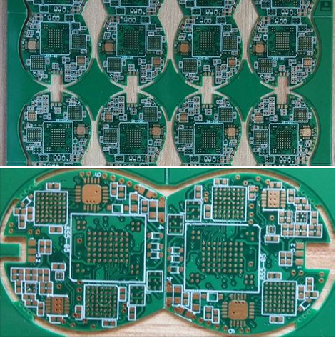
High Frequency Considerations In RF And Microwave Electronics Layout Design
In the rapidly advancing world of wireless communication, radar systems, and satellite technology, the design and layout of Radio Frequency (RF) and Microwave electronics stand as a critical frontier between theoretical performance and practical, reliable operation. While low-frequency circuit design often treats interconnections as ideal, zero-resistance paths, this assumption catastrophically fails at gigahertz frequencies. Here, the physical layout of components and traces on a printed circuit board (PCB) becomes an integral part of the circuit itself, directly influencing impedance, signal integrity, noise, and overall system efficiency. "High Frequency Considerations in RF and Microwave Electronics Layout Design" delves into the specialized principles and meticulous practices required to tame the electromagnetic behavior of circuits operating at these elevated frequencies. It bridges the gap between circuit theory and electromagnetic field theory, addressing the parasitic effects—unwanted capacitance, inductance, and radiation—that dominate performance. For engineers and designers, mastering these considerations is not merely an optimization step but a fundamental necessity to prevent a perfectly designed schematic from becoming a non-functional prototype, thereby ensuring signal fidelity, minimizing interference, and achieving the stringent performance targets demanded by modern high-speed applications.
Impedance Control and Transmission Line Theory
At the heart of RF layout design lies the imperative for controlled impedance. As signal wavelengths approach the physical dimensions of the PCB traces, these traces must be treated not as simple wires but as transmission lines. A transmission line is characterized by its per-unit-length inductance and capacitance, which together determine its characteristic impedance (typically 50 or 75 ohms). Maintaining a consistent impedance along the signal path from source to load is paramount to prevent signal reflections.
Reflections occur when there is an impedance discontinuity, causing portions of the signal to bounce back towards the source. This results in standing waves, signal distortion, and a severe degradation in power transfer. To avoid this, layout engineers meticulously calculate and design trace dimensions (width and thickness) relative to the PCB substrate's dielectric constant and height. This often involves using specific trace geometries like microstrip (a trace on an outer layer over a ground plane) or stripline (a trace embedded between two ground planes), each with its own equations and field confinement properties. Proper termination at the load, usually with a resistor matching the line's characteristic impedance, is essential to absorb the signal energy and eliminate reflections.
Grounding and Power Plane Strategies
Grounding in RF design is arguably more critical and complex than in digital or low-frequency analog design. An imperfect ground can introduce common-impedance coupling, ground loops, and act as an unintentional antenna. The primary goal is to provide a low-impedance return path for high-frequency currents, which requires a fundamentally different approach from the single-point grounding often used at lower frequencies.
A solid, unbroken ground plane is the gold standard in RF layouts. It serves as a universal reference plane, minimizes ground impedance, and provides shielding. For multilayer boards, dedicated ground layers are used. Vias must be placed frequently to stitch together ground planes on different layers, preventing them from resonating at certain frequencies. Similarly, power distribution requires careful planning. Power planes are often paired closely with adjacent ground planes to form a distributed decoupling capacitor, providing a low-impedance path for high-frequency noise. Strategic placement of multiple, small-value decoupling capacitors very close to IC power pins is crucial to suppress high-frequency transients and prevent noise from propagating through the power rail.
Component Selection, Placement, and Parasitics
Every physical component exhibits behavior beyond its ideal model at high frequencies. A simple wire, a resistor lead, or a capacitor's mounting pad introduces parasitic inductance and capacitance. These parasitics can cause a capacitor to become inductive above its self-resonant frequency or make a seemingly innocuous connection into a significant impedance. Therefore, component selection extends beyond nominal values to include package types (e.g., surface-mount devices, or SMDs, are vastly superior to through-hole parts), quality factors (Q), and self-resonant frequencies.
Placement is equally critical. The guiding principle is to minimize the length of all high-frequency current paths. This means placing critical components like amplifiers, filters, and oscillators as close together as possible. Long traces act as antennas and increase inductance. Sensitive nodes must be kept away from noisy ones. For instance, the output of a power amplifier should be physically isolated from the input of a low-noise amplifier to prevent oscillation or desensitization. Furthermore, component orientation can affect coupling; for example, adjacent inductors should be placed at right angles to minimize mutual magnetic coupling.
Shielding, Isolation, and Electromagnetic Compatibility (EMC)
At RF and microwave frequencies, circuits radiate and receive electromagnetic energy readily. Preventing unwanted emission (which can fail regulatory tests) and ensuring immunity from external interference are the dual goals of EMC. Layout is the first line of defense. Sensitive circuit blocks, such as local oscillators or low-noise input stages, are often isolated using shielding cans—metal enclosures soldered directly to the ground plane. These cans prevent radiative coupling between sections.
Isolation is also achieved through spatial separation and the use of guard rings—grounded traces that surround a sensitive trace or component to shunt away stray currents. Additionally, careful routing is essential: differential signaling can reject common-mode noise, and critical single-ended traces should be routed with adjacent ground traces (co-planar waveguide) for containment of fields. Filtering at every I/O connector, using ferrite beads and feedthrough capacitors, is standard practice to prevent noise from entering or leaving the board. A well-designed RF layout inherently considers the entire system as an electromagnetic entity, proactively managing fields rather than just currents.
Thermal Management and Material Selection
High-frequency circuits, particularly power amplifiers, generate significant heat. Excessive temperature degrades component performance, reduces reliability, and can cause thermal runaway. Effective thermal management must be integrated into the layout phase. This involves providing adequate thermal relief for heat-generating components, which often means connecting their thermal pads to large copper pours or internal ground planes using a grid of thermal vias. These vias conduct heat into the board's inner layers or to the opposite side where a heatsink can be attached.
The choice of PCB substrate material itself is a fundamental high-frequency consideration. Standard FR-4 material exhibits significant dielectric loss and poor consistency at frequencies above a few gigahertz. For microwave applications, specialized laminates with low dielectric loss (low loss tangent), stable dielectric constant over temperature and frequency, and tight manufacturing tolerances are used, such as Rogers, Teflon, or ceramic-filled materials. While more expensive, these materials ensure predictable performance, minimal signal attenuation, and stable impedance, which are non-negotiable for high-performance designs.

Mastering Multilayer PCB Stackup Design For Enhanced Electronic Performance
In the relentless pursuit of miniaturization, higher speeds, and greater functionality in modern electronics, the printed circuit board (PCB) has evolved far beyond a simple platform for component interconnection. At the heart of today's sophisticated devices lies the multilayer PCB, a complex laminate structure whose internal architecture—the stackup—is a critical determinant of overall system performance. Mastering multilayer PCB stackup design is no longer a secondary consideration but a foundational engineering discipline essential for achieving signal integrity, power integrity, electromagnetic compatibility (EMC), and thermal management. This article delves into the core principles and strategic considerations involved in crafting an optimal PCB stackup, moving beyond basic layer count to explore how deliberate material selection and layer ordering can dramatically enhance electronic performance, reliability, and manufacturability.
The Strategic Foundation: Defining Stackup Objectives and Constraints
Before a single layer is drawn, a successful stackup design begins with a clear understanding of the project's objectives and constraints. This phase involves defining the electrical, mechanical, and economic parameters that will guide all subsequent decisions. Key questions must be answered: What are the operating frequencies and data rates? What is the target impedance for critical signals? What are the power requirements and noise margins? Furthermore, mechanical constraints such as the final board thickness, the number of layers feasible within the budget, and the chosen fabrication capabilities of the PCB manufacturer must be established.
This initial planning sets the stage for all other stackup decisions. For instance, a high-speed digital design prioritizing signal integrity will have vastly different requirements than a dense, mixed-signal board containing sensitive analog circuits and RF components. Similarly, a design for a cost-sensitive consumer product may prioritize a minimal layer count, while a high-reliability aerospace application may emphasize robust power distribution and thermal dissipation, even at higher cost. By meticulously defining these goals upfront, designers can create a stackup that is not just functionally adequate but optimally tuned for its specific application.
Architecting for Signal Integrity: Controlled Impedance and Return Paths
Perhaps the most crucial role of the stackup is in preserving signal integrity, especially for high-speed digital and high-frequency analog circuits. A poorly designed stackup can lead to signal degradation, crosstalk, and timing errors that render a system unstable. The primary tools for managing signal integrity in the stackup are controlled impedance and the provision of clear, uninterrupted return paths for signals.
Controlled impedance is achieved by precisely designing the physical dimensions of a trace—its width and thickness—in relation to the dielectric material surrounding it and the distance to its reference plane (typically a ground or power plane). The stackup defines these dielectric heights (core and prepreg thicknesses) and the copper weights. Designers use these parameters in impedance calculators to determine trace geometries that match the required impedance (e.g., 50Ω or 100Ω differential). Consistency in these dielectric layers across the board is paramount for uniform impedance.
Equally important is the management of return currents. High-frequency signal currents return to their source via the path of least inductance, which is directly underneath the signal trace on an adjacent reference plane. A well-designed stackup ensures that every critical signal layer is adjacent to a solid reference plane. Breaking this plane with large splits or gaps forces the return current to find a longer, more inductive path, creating large current loops that radiate noise and increase susceptibility. Therefore, strategic pairing of signal and plane layers is a non-negotiable principle for maintaining clean signals and reducing electromagnetic emissions.
Powering the System: Robust Power Distribution Network (PDN) Design
The stackup is the physical embodiment of the Power Distribution Network (PDN). Its design directly impacts power integrity, which governs the stability of the voltage supplied to active components. A weak PDN, manifested as excessive impedance or noise on the power rails, can cause logic errors, reduced noise margins, and even component malfunction.
A fundamental strategy in stackup design is the use of dedicated power and ground plane pairs. Placing these planes closely together forms a natural, high-frequency decoupling capacitor due to the parallel plate capacitance between them. This inherent capacitance helps suppress high-frequency noise on the power rail, supplementing discrete decoupling capacitors. The stackup should be arranged to create multiple such plane pairs for different voltage levels, ensuring low-impedance power delivery across a broad frequency range.
Furthermore, the sequence of layers plays a role. Placing critical power planes adjacent to ground planes, and sandwiching high-speed signal layers between them, creates a shielded, stripline configuration. This not only contains the fields from the signals but also provides a stable reference for both the signals and the power. The strategic assignment of voltage layers and their proximity to ground directly influences the board's ability to deliver clean, stable power, especially during moments of high current demand when chips switch simultaneously.
Containing and Mitigating Electromagnetic Interference (EMI)
Electromagnetic Compatibility (EMC)—the ability of a device to function without causing or being susceptible to interference—is heavily dictated by PCB stackup design. The stackup is the first line of defense against both emitted radiation and external susceptibility. A thoughtful layer arrangement can act as a built-in shielding strategy.
The use of solid, unbroken ground planes is the most effective EMI control feature in a stackup. These planes provide shielding between signal layers, contain electromagnetic fields, and offer a low-impedance path for return currents, minimizing loop areas. As a rule, external signal layers should always be placed adjacent to a ground plane. If sensitive or high-speed traces must be on an outer layer, placing a ground plane directly underneath them is essential to contain their fields and reduce radiation.
For very noise-sensitive designs or those with stringent emission limits, a symmetric stackup around the board's centerline can be highly beneficial. Symmetry balances the inherent stresses in the laminated board, improving manufacturability and reducing the risk of warping. From an EMC perspective, a symmetric stackup with ground planes near the outer surfaces can create a "Faraday cage" effect, helping to contain internal noise. By carefully considering the placement of noisy and quiet circuit sections across layers and using planes as shields, designers can proactively mitigate EMI challenges long before a board is tested in an EMC chamber.
Material Selection and Fabrication Considerations
The performance of a brilliantly architected stackup can be undermined by inappropriate material choices. The dielectric materials, or laminates, used between copper layers have electrical and mechanical properties that directly impact performance. The key parameter is the dielectric constant (Dk or εr), which affects signal propagation speed and impedance. For consistent high-speed performance, a material with a stable Dk across frequency and temperature is critical. Loss tangent (Df) is another vital property, indicating how much signal energy is dissipated as heat; lower loss materials are essential for very high-frequency or long-distance transmission lines.
Beyond electrical properties, thermal and mechanical characteristics must align with the application. The Glass Transition Temperature (Tg) and Thermal Decomposition Temperature (Td) indicate a material's ability to withstand the heat of assembly (like lead-free soldering) and operation. Coefficient of Thermal Expansion (CTE) matching is crucial for reliability, especially when using large Ball Grid Array (BGA) components, to prevent solder joint failure over temperature cycles.
Finally, the stackup design must be translated into a manufacturable product. Close collaboration with the PCB fabricator during the stackup planning phase is invaluable. They can provide guidance on standard material thicknesses, available copper weights, and processing capabilities (like minimum dielectric spacing). Providing a complete stackup specification—including all material types, final thickness targets, and impedance requirements—ensures the fabricated board will match the design intent, turning a theoretical stackup into a high-performance reality.

Optimizing Component Placement And Routing In Modern PCB Layout Design
In the rapidly evolving landscape of electronics, the printed circuit board (PCB) remains the fundamental backbone, interconnecting components to bring a design to life. However, as devices become more powerful, compact, and complex, the task of laying out these boards has transformed from a simple connective exercise into a critical engineering discipline. Optimizing component placement and routing in modern PCB layout design is no longer a mere step in the process; it is the decisive factor between a high-performance, reliable product and one plagued by signal integrity issues, thermal problems, and manufacturing failures. This intricate dance of positioning components and tracing copper pathways directly influences electrical performance, electromagnetic compatibility (EMC), thermal management, manufacturability, and ultimately, the cost and time-to-market. For engineers and designers, mastering this optimization is the key to unlocking the full potential of today's advanced integrated circuits and high-speed interfaces, making it a compelling and essential field of study.
The Foundational Strategy: Intelligent Component Placement
The journey of optimization begins long before the first trace is drawn, with the strategic placement of every component on the board. This phase sets the stage for all subsequent routing and profoundly impacts the board's functionality. Effective placement starts with a logical grouping of components based on their functional blocks, such as power supply, microcontroller, memory, and RF sections. Keeping related components close together minimizes the overall trace lengths for critical signals, reducing parasitic inductance and capacitance that can degrade performance.
Beyond functional grouping, placement must account for mechanical and thermal constraints. Connectors, switches, and displays often have fixed locations dictated by the product enclosure. Large, heat-generating components like processors or power regulators must be positioned to facilitate heat dissipation, possibly near the board edge or directly under a heatsink. Furthermore, considering the assembly process is crucial. Placing components to enable efficient automated pick-and-place machine paths and ensuring adequate spacing for soldering and inspection tools can drastically reduce manufacturing defects and costs. A well-considered placement is a balanced compromise between electrical performance, physical constraints, and production practicality.
Navigating Electrical Performance: Signal and Power Integrity Routing
Once components are strategically placed, the focus shifts to the art and science of routing the copper traces that carry signals and power. For modern high-speed digital circuits and sensitive analog sections, routing is paramount for signal integrity. Critical signals, such as clock lines and differential pairs (e.g., USB, PCIe), require controlled impedance routing. This involves calculating and maintaining a specific trace width and spacing relative to the reference ground plane to achieve a target impedance, preventing signal reflections and ensuring clean data transmission.
Power integrity is equally vital. The power distribution network (PDN) must deliver stable, low-noise voltage to all components. This is achieved by using dedicated, wide power and ground planes within the PCB stack-up to provide low-impedance paths. For high-current paths, traces must be sufficiently wide to avoid excessive heating. Careful decoupling is also part of routing strategy; placing small bypass capacitors as close as possible to the power pins of ICs provides a local charge reservoir, suppressing high-frequency noise on the power rails. Proper routing for signal and power integrity ensures the electronic system operates reliably at its intended speed and power.
Ensuring Reliability: Thermal Management and EMC Considerations
A PCB that functions electrically but overheats or interferes with itself (or other devices) is a failure. Optimization must therefore integrate thermal management and electromagnetic compatibility (EMC) from the ground up. Thermally, routing can help by using thicker copper or dedicated copper pours (fills) on outer layers to act as heat spreaders, drawing heat away from hot components. Strategic placement of thermal vias—an array of plated holes—under a component's thermal pad can conduct heat efficiently to inner ground planes or a dedicated back-side heatsink.
For EMC, the goal is to minimize both the emission of and susceptibility to electromagnetic interference. A fundamental practice is maintaining a continuous, unbroken ground plane, which provides a shield and a return path for signals. High-speed traces should be routed over this solid ground plane, and sensitive traces must be kept away from noise sources like switching power supplies or clock generators. For particularly noisy sections, guard traces—grounded traces running parallel to a sensitive line—or even full shielding cans may be necessary. By proactively designing for thermal and EMC performance during placement and routing, designers prevent costly board spins and compliance testing failures later.
Leveraging Modern Tools and Design for Manufacturing
The complexity of modern PCB optimization is untenable without sophisticated electronic design automation (EDA) software. These tools are indispensable partners, offering features like real-time design rule checking (DRC), which enforces constraints for trace width, spacing, and layer usage. Auto-routers have evolved, but their most effective use is often for completing non-critical connections after the designer has manually routed the critical, high-speed paths. More advanced tools provide simulation capabilities for signal integrity, power integrity, and thermal analysis, allowing designers to virtual prototype and refine their layout before fabrication.
Finally, all optimization must be validated through the lens of Design for Manufacturing (DFM) and Design for Assembly (DFA). This means adhering to the fabricator's capabilities regarding minimum trace/space, hole sizes, and copper-to-edge clearance. It involves creating clear solder mask layers to prevent bridging and providing a comprehensive silkscreen for assembly identification. A design that is electrically perfect but cannot be reliably built is not optimized. The ultimate goal is a layout that achieves peak performance while being robust, cost-effective, and straightforward to manufacture at scale, seamlessly bridging the gap between digital design and physical reality.
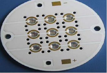
Modern Light Dimming Control Features Enabling Personalized Brightness Levels In Any Room
Technological Foundations and Smart Integration
The core of modern dimming lies in its advanced technological underpinnings. Unlike older phase-cut dimmers that often caused flickering or humming with incompatible LED bulbs, contemporary systems utilize digital protocols like DALI (Digital Addressable Lighting Interface), DMX, or wireless standards such as Zigbee, Z-Wave, and Wi-Fi. These protocols enable precise, granular control over each light fixture's intensity, often down to 1% increments, ensuring smooth, flicker-free dimming across a wide range of light sources, from LEDs to halogen.
Integration with smart home platforms is a game-changer. Systems can be managed via centralized hubs, voice assistants like Amazon Alexa or Google Assistant, or intuitive smartphone apps. This connectivity allows users to create and schedule lighting scenes—for instance, a "Morning" scene with bright, cool light to energize, or an "Evening Relaxation" scene with warm, subdued tones. Moreover, these systems can interact with other smart devices; lights can dim automatically when a smart TV is turned on, or brighten when a motion sensor detects activity, creating a truly interconnected and automated living environment.
Enhancing Human Health and Well-being
One of the most significant impacts of personalized dimming is on human health, particularly through alignment with circadian rhythms. Our biological clocks are heavily influenced by light intensity and color temperature. Modern dimming systems, often coupled with tunable white technology, can automatically adjust brightness and color throughout the day—emulating the natural progression of sunlight. Bright, blue-enriched light in the morning promotes alertness, while gradually dimming, warmer light in the evening signals the body to produce melatonin, aiding relaxation and sleep.
Beyond circadian support, personalized control addresses individual sensory needs and tasks. For someone with photophobia or migraines, the ability to finely tune brightness to a comfortable level can be life-changing. In a home office, a user might increase brightness for detailed work and lower it for video calls to reduce screen glare. This adaptability reduces eye strain, minimizes fatigue, and creates environments that support both mental focus and physical comfort, contributing to overall long-term well-being.
Energy Efficiency and Environmental Sustainability
Modern dimming is a powerful tool for energy conservation. Reducing light output by just 25% can save approximately 20% in energy consumption, as power usage in LEDs is nearly proportional to light output. Smart dimming systems take this further with automated features like occupancy sensing and daylight harvesting. Lights can dim or turn off in unoccupied rooms, and sensors can measure ambient natural light and adjust artificial lighting accordingly to maintain a consistent, desired light level without waste.
This efficiency translates directly into environmental benefits. By lowering electricity demand, these systems reduce the carbon footprint of a building. Furthermore, by operating LEDs at lower, optimized intensities, their lifespan is significantly extended, reducing electronic waste from frequent bulb replacements. When implemented on a large scale in commercial or municipal settings, intelligent dimming contributes substantially to broader sustainability goals and green building certifications like LEED.
Aesthetic Flexibility and Architectural Enhancement
Lighting is a fundamental element of interior design, and modern dimming provides unparalleled creative freedom. Designers and homeowners can use light to sculpt a space, highlight architectural features, or create specific moods. With zonal and individual fixture control, different areas within an open-plan room can have distinct lighting atmospheres—a brightly lit kitchen island alongside a softly illuminated dining area, for example.
This technology enables dynamic lighting scenes that can transform a room's character instantly. A living room can shift from a vibrant, uniform brightness for social gatherings to a layered, dramatic setup with accent lighting on artwork for a more intimate evening. The precision of dimming allows for perfect balance, eliminating shadows where they are unwanted and creating them for effect where desired. This turns static architecture into an interactive canvas, where light itself becomes a decorative and functional medium that can be personalized for every occasion.
Accessibility and Inclusive Design
Personalized dimming control is a cornerstone of inclusive and accessible design. For elderly individuals or those with limited mobility, voice control or simple tablet interfaces eliminate the need to reach for physical switches. Preset scenes can be programmed for common activities, making the environment easier and safer to navigate.
Furthermore, these systems can be tailored to support individuals with visual impairments or neurological conditions such as autism, who may have specific lighting sensitivities. The ability to create and recall personalized, consistent lighting environments reduces anxiety and increases independence. In public spaces and workplaces, offering user-controlled lighting at individual workstations or in hotel rooms demonstrates a commitment to universal design, ensuring comfort and usability for the widest possible range of people, thereby fostering a more equitable and comfortable built environment for all.
REPORT


