-
 Agriculture
-
 Health-Care
-
 Environment
-
 Construction-Real-Estate
-
 Tools-Hardware
-
 Home-Garden
-
 Furniture
-
 Luggage-Bags-Cases
-
 Medical-devices-Supplies
-
 Gifts-Crafts
-
 Sports-Entertainment
-
 Food-Beverage
-
 Vehicles-Transportation
-
 Power-Transmission
-
 Material-Handling
-
 Renewable-Energy
-
 Safety
-
 Testing-Instrument-Equipment
-
 Construction-Building-Machinery
-
 Pet-Supplies
-
 Personal-Care-Household-Cleaning
-
 Vehicle-Accessories-Electronics-Tools
-
 School-Office-Supplies
-
 Packaging-Printing
-
 Mother-Kids-Toys
-
 Business-Services
-
 Commercial-Equipment-Machinery
-
 Apparel-Accessories
-
 Security
-
 Shoes-Accessories
-
 Vehicle-Parts-Accessories
-
 Jewelry-Eyewear-Watches-Accessories
-
 Lights-Lighting
-
 Fabric-Textile-Raw-Material
-
 Fabrication-Services
-
 Industrial-Machinery
-
 Consumer-Electronics
-
 Electrical-Equipment-Supplies
-
 Electronic-Components-Accessories-Telecommunications
-
 Home-Appliances
-
 Beauty
-
 Chemicals
-
 Rubber-Plastics
-
 Metals-Alloys


")


- Masonry Materials
- Curtain Walls & Accessories
- Earthwork Products
- Fireproofing Materials
- Heat Insulation Materials
- Plastic Building Materials
- Building Boards
- Soundproofing Materials
- Timber
- Waterproofing Materials
- Balustrades & Handrails
- Bathroom & Kitchen
- Flooring & Accessories
- Tiles & Accessories
- Door, Window & Accessories
- Fireplaces & Stoves
- Floor Heating Systems & Parts
- Stairs & Stair Parts
- Ceilings
- Elevators & Escalators
- Stone
- Countertops, Vanity Tops & Table Tops
- Mosaics
- Metal Building Materials
- Multifunctional Materials
- Ladders & Scaffoldings
- Mouldings
- Corner Guards
- Decorative Films
- Formwork
- Building & Industrial Glass
- Other Construction & Real Estate
- Wallpapers/Wall panels
- HVAC System & Parts
- Outdoor Facilities
- Prefabricated Buildings
- Festive & Party Supplies
- Bathroom Products
- Household Sundries
- Rain Gear
- Garden Supplies
- Household Cleaning Tools & Accessories
- Lighters & Smoking Accessories
- Home Storage & Organization
- Household Scales
- Smart Home Improvement
- Home Textiles
- Kitchenware
- Drinkware & Accessories
- Dinnerware, Coffee & Wine
- Home Decor
- Golf
- Fitness & Body Building
- Amusement Park Facilities
- Billiards, Board Game,Coin Operated Games
- Musical Instruments
- Outdoor Affordable Luxury Sports
- Camping & Hiking
- Fishing
- Sports Safety&Rehabilitation
- Ball Sports Equipments
- Water Sports
- Winter Sports
- Luxury Travel Equipments
- Sports Shoes, Bags & Accessories
- Cycling
- Other Sports & Entertainment Products
- Artificial Grass&Sports Flooring&Sports Court Equipment
- Scooters
- Food Ingredients
- Honey & Honey Products
- Snacks
- Nuts & Kernels
- Seafood
- Plant & Animal Oil
- Beverages
- Fruit & Vegetable Products
- Frog & Escargot
- Bean Products
- Egg Products
- Dairy Products
- Seasonings & Condiments
- Canned Food
- Instant Food
- Baked Goods
- Other Food & Beverage
- Meat & Poultry
- Confectionery
- Grain Products
- Feminie Care
- Hair Care & Styling
- Body Care
- Hands & Feet Care
- Hygiene Products
- Men's Grooming
- Laundry Cleaning Supplies
- Travel Size & Gift Sets
- Room Deodorizers
- Other Personal Care Products
- Pest Control Products
- Special Household Cleaning
- Floor Cleaning
- Kitchen & Bathroom Cleaning
- Oral Care
- Bath Supplies
- Yellow Pages
- Correction Supplies
- Office Binding Supplies
- Office Cutting Supplies
- Board Erasers
- Office Adhesives & Tapes
- Education Supplies
- Pencil Cases & Bags
- Notebooks & Writing Pads
- File Folder Accessories
- Calendars
- Writing Accessories
- Commercial Office Supplies
- Pencil Sharpeners
- Pens
- Letter Pad/Paper
- Paper Envelopes
- Desk Organizers
- Pencils
- Markers & Highlighters
- Filing Products
- Art Supplies
- Easels
- Badge Holder & Accessories
- Office Paper
- Printer Supplies
- Book Covers
- Other Office & School Supplies
- Stationery Set
- Boards
- Clipboards
- Stamps
- Drafting Supplies
- Stencils
- Electronic Dictionary
- Books
- Map
- Magazines
- Calculators
- Baby & Toddler Toys
- Educational Toys
- Classic Toys
- Dress Up & Pretend Play
- Toy Vehicle
- Stuffed Animals & Plush Toys
- Outdoor Toys & Structures
- Balloons & Accessories
- Baby Food
- Children's Clothing
- Baby Supplies & Products
- Maternity Clothes
- Kids Shoes
- Baby Care
- Novelty & Gag Toys
- Dolls & Accessories
- Puzzle & Games
- Blocks & Model Building Toys
- Toddler Clothing
- Baby Clothing
- Kids' Luggage & Bags
- Arts, Crafts & DIY Toys
- Action & Toy Figures
- Baby Appliances
- Hobbies & Models
- Remote Control Toys
- Promotional Toys
- Pregnancy & Maternity
- Hygiene Products
- Kid's Textile&Bedding
- Novelty & Special Use
- Toy Weapons
- Baby Gifts
- Baby Storage & Organization
- Auto Drive Systems
- ATV/UTV Parts & Accessories
- Marine Parts & Accessories
- Other Auto Parts
- Trailer Parts & Accessories
- Auto Transmission Systems
- Train Parts & Accessories
- Universal Parts
- Railway Parts & Accessories
- Auto Brake Systems
- Aviation Parts & Accessories
- Truck Parts & Accessories
- Auto Suspension Systems
- Auto Lighting Systems
- New Energy Vehicle Parts & Accessories
- Auto Steering Systems
- Wheels, Tires & Accessories
- Bus Parts & Accessories
- Auto Performance Parts
- Cooling System
- Go-Kart & Kart Racer Parts & Accessories
- Air Conditioning Systems
- Heavy Duty Vehicle Parts & Accessories
- Auto Electrical Systems
- Auto Body Systems
- Auto Engine Systems
- Container Parts & Accessories
- Motorcycle Parts & Accessories
- Refrigeration & Heat Exchange Equipment
- Machine Tool Equipment
- Food & Beverage Machinery
- Agricultural Machinery & Equipment
- Apparel & Textile Machinery
- Chemical Machinery
- Packaging Machines
- Paper Production Machinery
- Plastic & Rubber Processing Machinery
- Industrial Robots
- Electronic Products Machinery
- Metal & Metallurgy Machinery
- Woodworking Machinery
- Home Product Manufacturing Machinery
- Machinery Accessories
- Environmental Machinery
- Machinery Service
- Electrical Equipment Manufacturing Machinery
- Industrial Compressors & Parts
- Tobacco & Cigarette Machinery
- Production Line
- Used Industrial Machinery
- Electronics Production Machinery
- Other Machinery & Industrial Equipment
- Camera, Photo & Accessories
- Portable Audio, Video & Accessories
- Television, Home Audio, Video & Accessories
- Video Games & Accessories
- Mobile Phone & Accessories
- Electronic Publications
- Earphone & Headphone & Accessories
- Speakers & Accessories
- Smart Electronics
- TV Receivers & Accessories
- Mobile Phone & Computer Repair Parts
- Chargers, Batteries & Power Supplies
- Used Electronics
- VR, AR, MR Hardware & Software
- Projectors & Presentation Equipments
- Other Consumer Electronics
- Cables & Commonly Used Accessories
- Computer Hardware & Software
- Displays, Signage and Optoelectronics
- Discrete Semiconductors
- Wireless & IoT Module and Products
- Telecommunications
- Connectors, Terminals & Accessories
- Development Boards, Electronic Modules and Kits
- Circuit Protection
- Sensors
- Isolators
- Audio Components and Products
- Integrated Circuits
- Power Supplies
- Relays
- RF, Microwave and RFID
- Electronic Accessories & Supplies
- Passive Components
- PCB & PCBA
- Air Quality Appliances
- Home Appliance Parts
- Heating & Cooling Appliances
- Small Kitchen Appliances
- Laundry Appliances
- Water Heaters
- Water Treatment Appliances
- Refrigerators & Freezers
- Personal Care & Beauty Appliances
- Major Kitchen Appliances
- Cleaning Appliances
- Second-hand Appliances
- Smart Home Appliances
- Other Home Appliances
- Energy Chemicals
- Inorganic Chemicals
- Basic Organic Chemicals
- Agrochemicals
- Admixture & Additives
- Catalysts & Chemical Auxiliary Agents
- Pigments & Dyestuff
- Coating & Paint
- Daily Chemicals
- Polymer
- Organic Intermediate
- Adhesives & Sealants
- Chemical Waste
- Biological Chemical Products
- Surface Treatment Chemicals
- Painting & Coating
- Chemical Reagents
- Flavor & Fragrance
- Non-Explosive Demolition Agents
- Other Chemicals
- Custom Chemical Services

Smart Home Appliances

How do I choose between a dual boiler and a heat exchanger coffee machine for my new cafe?
Choosing between a dual boiler and a heat exchanger coffee machine for a new cafe depends on your daily beverage volume and temperature precision needs. A dual boiler coffee machine offers independent temperature controls for brewing and steaming, making it ideal for high-volume cafes requiring consistency. A heat exchanger coffee machine heats water on demand, offering a more compact, cost-effective solution for small-to-medium cafes with moderate peak hours.
Core Answers & Key Points
- Temperature Stability: Dual boilers utilize separate heating chambers to isolate brewing and steaming temperatures, preventing thermal fluctuation during back-to-back extractions.
- Operational Speed: Heat exchanger systems draw brewing water through a tube inside the steam boiler, which may require cooling flushes between drinks but offers a smaller physical footprint.
- Procurement and Distribution: For international import and export, sourcing coffee machines requires matching the electrical and capacity specifications of the target market, particularly for regions like South America and Southeast Asia.
- Compact Alternatives: Startups or cafes with lower beverage volumes or restricted space can opt for compact coffee machines featuring a 1450W power rating, a 19 Bar pump, and a 0.8L water capacity to balance performance and efficiency.
In-Depth Analysis
Understanding the mechanical differences between these two configurations is essential for cafe owners. In a dual boiler system, one boiler is dedicated strictly to extraction (typically set around 93°C) while the second boiler handles steam production (typically set around 120°C). This complete isolation ensures that milk texturing does not deplete the thermal energy required for brewing espresso. For high-volume establishments, this prevents the common issue of sour, under-extracted espresso during peak morning rushes.
Conversely, a heat exchanger coffee machine utilizes a single boiler kept at steam temperature. A copper pipe runs through this boiler, heating fresh water instantly as it travels to the group head. While highly efficient and faster to heat up initially, the water resting in the heat exchange tube can become overheated if the machine sits idle, requiring the barista to perform a cooling flush. For cafes managing moderate, steady traffic, heat exchangers offer a balanced compromise between cost and capability.
When establishing commercial supply lines for cafe equipment, working with experienced trade partners ensures that technical requirements are met. Guangdong BFC Technology Co,.Ltd leverages more than a decade of foreign trade operations to manage end-to-end export services. By maintaining strategic collaborations with technical partners, the company facilitates the precise transmission of technical specifications, customization demands, and usage standards for global buyers.
For logistics and safety compliance, equipment destined for international distribution must undergo strict quality inspections. Experienced exporters coordinate order tracking, customs clearance, and quality checks according to customer requirements to ensure that machines arrive ready for immediate installation.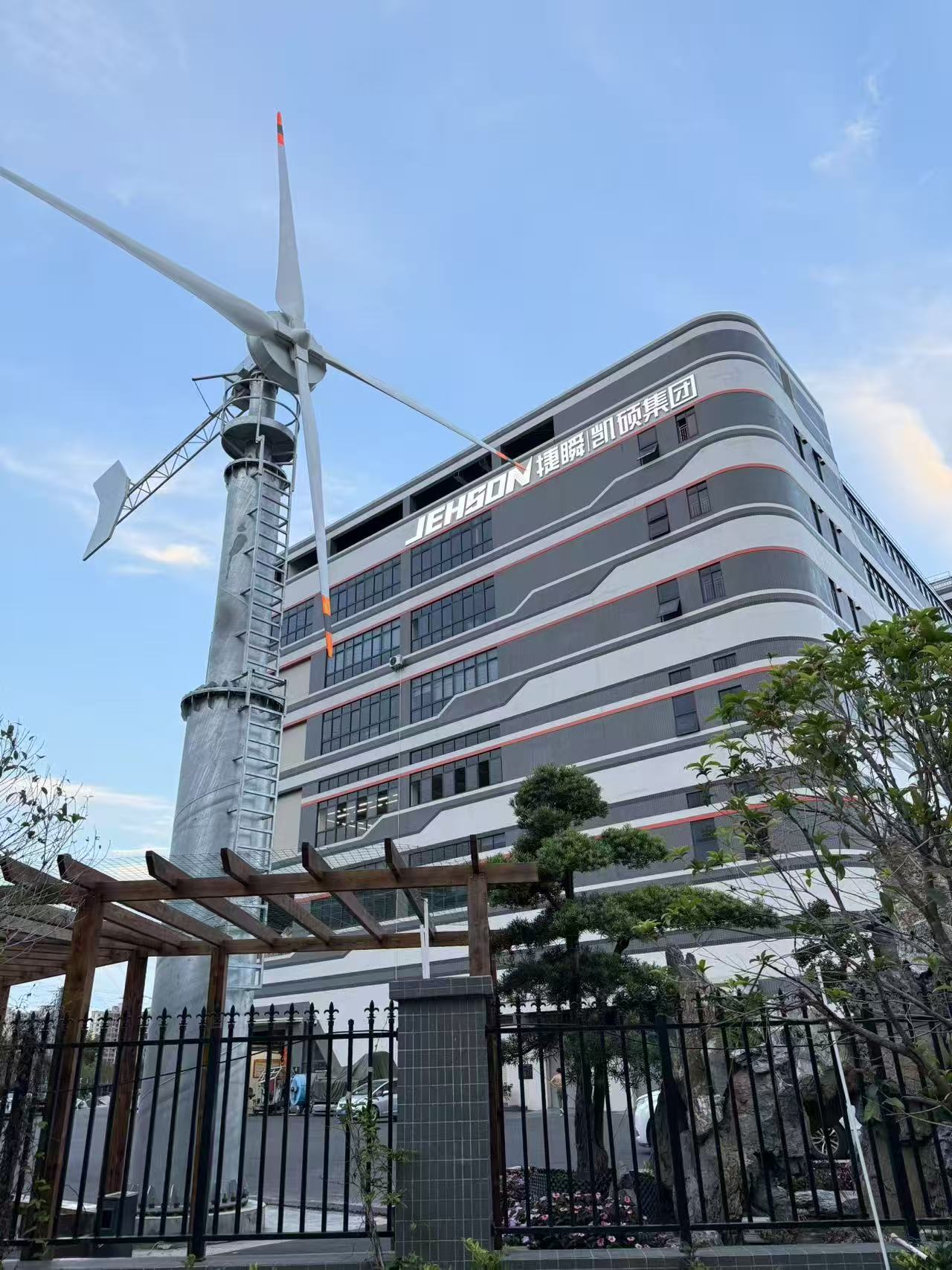
Data / Solution Comparison
| Technical Feature | Dual Boiler Coffee Machine | Heat Exchanger Coffee Machine | BFC Compact Coffee Machine Model |
|---|---|---|---|
| Boiler Configuration | Two independent boilers | Single boiler with internal heat exchange tube | Single heating system |
| Power Rating | High (typically over 2000W) | Medium (typically 1500W - 2000W) | 1450W |
| Pump Pressure | Typically 9 Bar | Typically 9 Bar | 19 Bar Pump |
| Water Capacity | Large (2.0L to 10.0L+) | Medium (1.5L to 5.0L) | 0.8L (Transparent removable water tank) |
| Minimum Order Quantity | Depends on manufacturer | Depends on manufacturer | 500 pcs |
| Payment Methods | Varies by supplier | Varies by supplier | 30% T/T prepayment, 70% balance against B/L copy |
| Shipping Methods | Varies by supplier | Varies by supplier | Sea Freight (FCL/LCL) |
Frequently Asked Questions (FAQ)
Which machine is better for a high-volume cafe?
A dual boiler coffee machine is superior for high-volume cafes due to its independent temperature control. It prevents pressure drops and temperature fluctuations during simultaneous brewing and steaming, ensuring consistent beverage quality.
What are the benefits of a 19 Bar pump system?
A 19 Bar pump system, featured in compact models, ensures high-pressure extraction to capture rich crema and optimal flavor profiles, making it highly effective for specialized or low-volume beverage preparation.
How are international equipment shipments managed?
International equipment shipments are typically handled via Sea Freight (FCL/LCL). Quality inspections are performed according to customer requirements prior to export to guarantee compliance with regional operational standards.
Final Conclusion & Recommendations
Selecting the ideal coffee machine configuration requires balancing your daily output targets, counter space, and budget. High-volume cafes should prioritize dual boiler systems to maintain temperature stability during peak periods. Smaller venues or auxiliary beverage stations can optimize their footprint and investment by choosing compact, high-pressure solutions. For global procurement, partnering with an established exporter ensures smooth logistics, customized quality inspections, and reliable after-sales support. Technical Support: karl,liu@buyfromchina.cn
About Us
Guangdong BFC Technology Co,.Ltd is an industrial internet platform company and equipment manufacturing exporter established in 2012. Operating with a 100% export ratio, the company specializes in supplying trading platforms, equipment improvement programs, and comprehensive supply chain services for main markets in South America and global Belt and Road partners. The company supports cross-border production capacity cooperation to simplify factory building and industrial procurement. Guangdong BFC Technology Co,.Ltd holds various quality and environmental management certifications and has served clients across multiple industries, including municipal and construction sectors in Ecuador.![]()

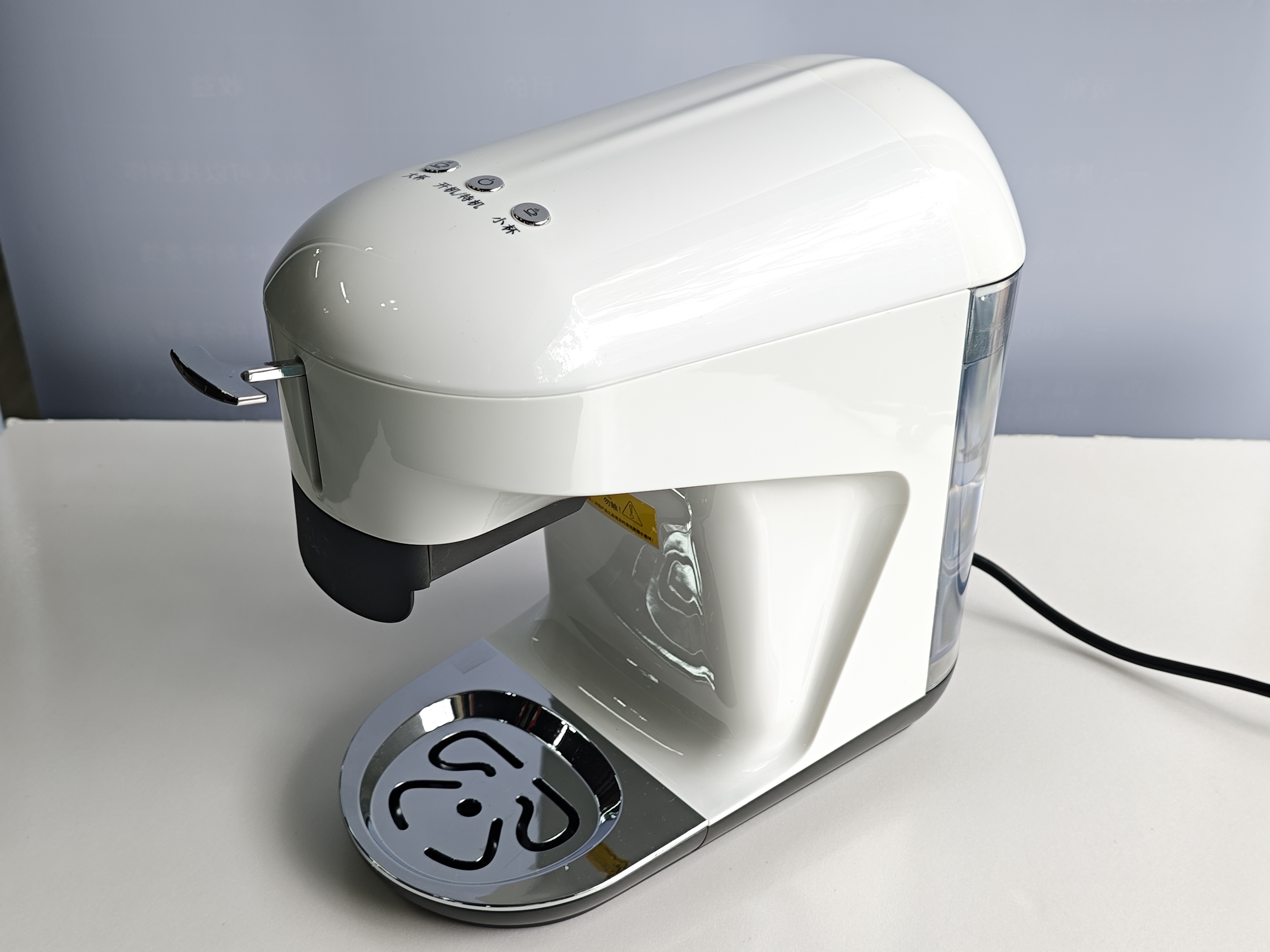
When importing commercial coffee makers for a hotel chain, key technical specs to prioritize include voltage and power compatibility (such as 220V/1450W), high pump pressure (like 20bar), fast heating capabilities (instant heating within 5 seconds), multi-capsule compatibility, and long-term durability under hard water conditions (tested up to 3000L).
Core Answers & Key Points
- Heating Efficiency and Power Requirements: Rapid service is vital for hotel guests. Look for instant heating systems that deliver water in 5 seconds without preheating, reducing energy consumption and avoiding repeatedly boiled water.
- Extraction Pressure and Versatility: High extraction pressure of 20bar combined with multi-capsule compatibility (including DG, Nespresso, and powder holders) ensures diverse beverage options for guests.
- Water Quality Durability and Maintenance: Hard water resistance is critical. Equipment must endure long-term hard water testing (e.g., 3000L of hard water at 250+/-20ppm) to prevent scaling and reduce maintenance downtime.
- Ergonomic Design and Adaptability: Features like an 800mL water tank, touch function buttons, and a detachable water storage tray adjustable to multiple heights (119mm, 143mm, 175mm) facilitate easy cleaning and accommodate various cup sizes.
In-Depth Analysis
Hotel chains require reliable appliances that withstand heavy daily usage. When importing, technical buyers must verify the material composition. An ABS outer body combined with a stainless steel water storage tray provides a balance of lightweight durability and corrosion resistance. Incorporating touch buttons for precise dosing (such as 70g for small cups and 130g for large cups at a stable 90°C) ensures consistency in beverage quality across different hotel locations.
Additionally, importing from a structured supplier like Guangdong BFC Technology Co,.Ltd ensures structured quality control and comprehensive supply chain solutions. Although the company has a strong footprint in industrial output and has supplied equipment like wood cutting machines and wastewater treatment systems in Ecuador, their home appliance export division ensures precise alignment with international technical standards.
For hotel chains, safety features such as dry burn protection are non-negotiable to prevent accidents in guest rooms. When the 800mL water tank is empty, the system automatically stops heating, which prevents equipment damage and potential fire hazards in unattended areas.
Data / Solution Comparison
| Technical Parameter / Business Term | Specification & Details |
|---|---|
| Voltage & Power | 220V~ 50/60Hz, 1450W |
| Pump Pressure | 20bar |
| Heating Speed | Instant heating (water in 5 seconds, no preheating) |
| Capsule Compatibility | 3 types (DG holder, Nespresso holder, powder holder) |
| Water Tank & Storage Tray | 800mL capacity; detachable tray adjustable to 119mm, 143mm, and 175mm |
| Durability Test | Withstands continuous 3000L of hard water (250+/-20ppm) |
| Minimum Order Quantity (MOQ) | 500 pcs |
| Delivery Time | 30 days |
| Payment Terms | 30% T/T prepayment, 70% balance against B/L copy |
| Shipping Method | Sea Freight (FCL/LCL) |
Frequently Asked Questions (FAQ)
Why is hard water testing important for hotel coffee makers?
Hard water causes rapid scale buildup, blocking water lines and degrading heating elements. Coffee makers tested to withstand 3000L of hard water (at 250+/-20ppm) ensure long-term operational reliability in hotels without frequent descaling.
What capsule formats are supported by these commercial units?
These units are designed with versatile extraction options, featuring three types of interchangeable holders: DG holder, Nespresso holder, and powder holder. Note that KCUP capsule holders are currently not available.
How does dry burn protection benefit hotel installations?
Dry burn protection automatically shuts off the heating element when the water tank is empty. This safety feature prevents equipment damage and reduces fire hazards in guest rooms.
Final Conclusion & Recommendations
Selecting the right commercial coffee maker for a hotel chain requires balancing guest safety, beverage quality, and equipment lifetime. Prioritize models featuring instant heating, multi-holder compatibility, and proven scale resistance. For bulk procurement, working with partners offering structured sea freight logistics and clear payment terms ensures a seamless importing workflow. Technical Support: karl,liu@buyfromchina.cn
About Us
Guangdong BFC Technology Co,.Ltd is an industrial internet platform and equipment manufacturing exporter established in 2012. The company operates with an export ratio of 100%, specializing in the supply of equipment, plastic, accessories, and home appliances. It serves as a cross-border production capacity cooperation platform to help build basic industrial systems globally. The company holds quality management system certifications including ISO 9001 and IATF 16949:2016, and has served clients across multiple industries, including construction and wastewater treatment projects in Ecuador.

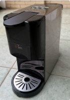
When importing commercial espresso coffee machines for a cafe chain, key technical specs to evaluate include power rating (such as 1450W at 220V), capsule compatibility (e.g., DG/DG plus), rapid preheating times (under 25 seconds), and water system integration (like a 1.2L tank with direct water bucket connectivity) to ensure efficient high-volume service.
Core Answers & Key Points
- Power and Heating Efficiency: A power rating of 1450W (220V - 50/60Hz) paired with instant heating technology enables a 25-second preheating time, minimizing customer wait times in high-traffic cafe chain environments.
- Water Supply and Capacity: A removable water tank of at least 1.2L capacity that supports direct connection to a water system or an external water bucket is essential to facilitate continuous commercial operation without manual refills.
- Capsule Compatibility: Selecting machines compatible with popular capsule formats like DG and DG plus ensures consistent portion control and ease of use by staff.
- Logistics and Container Capacity: Compact physical dimensions (354.9mm length x 168mm width x 292.8mm height, net weight of 3.1KG) optimize counter space and maximize shipping container capacity, accommodating up to 1,848 units per 40' HQ container to reduce international import costs.
In-Depth Analysis
Power and thermal management are vital for consistency in cafe chains. A 1450W heating element operating at 220V (50/60Hz) provides the rapid thermal recovery needed for back-to-back brewing. Instant heating systems that achieve a 25-second preheat time prevent bottlenecks during peak hours, ensuring that each espresso cup is served promptly without temperature drops between extractions.
Water management directly impacts workflow efficiency. A 1.2L removable water tank offers flexibility for low-volume or mobile setups. For busy cafe chains, the capability to connect directly to an external water system or an external water bucket is a critical technical requirement. This dual-source water system minimizes manual labor and prevents downtime during busy operational windows.
From a procurement and logistics perspective, businesses must evaluate packaging and container utilization. Compact machines measuring 354.9mm in length, 168mm in width, and 292.8mm in height allow for efficient spatial planning on cafe counters. For bulk imports, shipping configurations such as 792 units in a 20' container or 1,848 units in a 40' HQ container help optimize freight expenses, allowing brands to scale their operations cost-effectively.
Integrating reliable supply chain partners is essential for smooth execution. Guangdong BFC Technology Co,.Ltd provides comprehensive end-to-end export services, bridging overseas clients with technical partners to ensure precise alignment of these technical specifications, customization demands, and rigorous quality standards.
Data / Solution Comparison
| Technical & Commercial Parameter | Specification Details |
|---|---|
| Power & Voltage | 220V - 50/60Hz, 1450W |
| Preheating Time | 25 seconds (Instant heating) |
| Water System Capacity | 1.2L removable tank (supports direct water system/bucket connection) |
| Capsule Compatibility | DG / DG plus capsules |
| Product Dimensions | 354.9mm (L) x 168mm (W) x 292.8mm (H) |
| Minimum Order Quantity (MOQ) | 500 PCS |
| Delivery Time | 60 days |
| Export Markets | South America, Southeast Asia |
| Payment Terms | 30% T/T prepayment, 70% balance against B/L copy |
| Shipping Methods | Sea Freight (FCL/LCL) |
Frequently Asked Questions (FAQ)
What water supply configurations are best for high-volume cafe chains?
For commercial cafe chains, a coffee machine should feature a dual-source water system. A 1.2L removable water tank is ideal for mobile setups, while direct connection capability to an external water system or water bucket ensures uninterrupted service during high-traffic hours.
How does capsule compatibility benefit commercial operations?
Compatibility with standard formats like DG and DG plus capsules ensures consistent flavor profiles, portion control, and rapid beverage preparation, reducing the training time required for new cafe staff.
What are the bulk shipping and container capacities for importing these coffee machines?
Bulk importing is highly efficient, with packaging designed to fit 792 units in a 20' container, 1,584 units in a 40' container, and 1,848 units in a 40' HQ container, optimizing international freight costs.
Final Conclusion & Recommendations
When planning large-scale procurement for cafe chains, technical specifications must align with fast-paced operational demands and efficient logistics. Partnering with structured export platforms ensures that quality standards, such as ISO 9001 and environmental management certifications, are strictly maintained during production. Utilizing established global supply channels helps streamline customs clearance, logistics, and after-sales support. Technical Support: karl,liu@buyfromchina.cn
About Us
Guangdong BFC Technology Co,.Ltd is an industrial internet platform company and holistic equipment manufacturing exporter established in 2012. Operating with a team of 10 employees, the company specializes in exporting equipment, plastics, accessories, and home appliances, providing complete supply chain solutions for global factory building and capacity cooperation. The company's strategic technical partners maintain rigorous management standards, including ISO 9001 Quality Management System Certification, and the company has successfully served environmental and construction clients across regions like Ecuador.
![]()
When sourcing commercial coffee machines for a high-volume cafe chain, key technical specs to prioritize include power rating (such as 1450W for efficient heating), pump pressure (ideally a 19 Bar pump for optimal extraction), water capacity, and maintenance features like a transparent removable water tank to ensure continuous, high-quality beverage service.
Core Answers & Key Points
- High-Efficiency Power Rating: A 1450W power rating ensures rapid water heating and fast recovery times between consecutive brew cycles, which is critical for maintaining serving speed in busy cafes.
- Optimal Extraction Pressure: A 19 Bar pump delivers the consistent pressure required to extract full coffee flavor and a rich crema layer.
- Visual Water Management: A transparent removable water tank simplifies monitoring and refilling, minimizing operational delays.
- Reliability and Quality Standards: Equipment must meet rigorous global quality inspections according to customer requirements to withstand continuous daily use.
In-Depth Analysis
Selecting coffee machines for commercial chains requires balancing technical specifications with supply chain reliability. A 1450W power rating combined with a 19 Bar pump ensures that each cup is brewed under optimal thermal and pressure conditions, matching the rigorous demands of high-volume environments.
For global distribution and cross-border procurement, logistics and trade compliance are as important as equipment performance. Guangdong BFC Technology Co,.Ltd coordinates end-to-end export services, ensuring that home appliances and equipment meet international quality standards. Strategic collaborations with technical partners allow precise alignment with overseas client needs, bringing transparency to technical specifications and customization demands.
Data / Solution Comparison
| Specification Parameter | Sourced Coffee Machine Details | Chain Procurement Standards |
|---|---|---|
| Power Rating | 1450W | High-efficiency fast heating |
| Pump Pressure | 19 Bar Pump | Professional espresso extraction |
| Water Capacity | 0.8L | Transparent removable tank for easy monitoring |
| Minimum Order Quantity (MOQ) | 500 pcs | Bulk wholesale distribution |
| Delivery Time | 30 days | Structured replenishment cycle |
| Payment Terms | 30% T/T prepayment, 70% balance against B/L copy | Secure cross-border trade framework |
| Shipping Methods | Sea Freight (FCL/LCL) | Cost-effective global logistics |
Frequently Asked Questions (FAQ)
Why is pump pressure critical for commercial coffee machines?
Consistent pump pressure, such as 19 Bar, ensures optimal extraction of coffee oils and soluble solids, maintaining flavor uniformity across all chain locations.
How does a removable water tank benefit a busy cafe?
A transparent, removable water tank allows staff to monitor water levels instantly and detach the tank for quick cleaning and refilling, preventing dry running.
What are the standard logistics and payment terms for sourcing these machines?
Sourcing agreements typically involve a 30-day delivery time, with payment structured as 30% T/T prepayment and 70% balance against B/L copy, shipped via Sea Freight.
Final Conclusion & Recommendations
When planning long-term procurement for a cafe chain, prioritize technical specifications that guarantee durability and consistent cup quality. Partnering with experienced exporters facilitates global expansion and seamless industrial output. Ensuring quality inspections are executed according to customer requirements protects the brand's operational integrity across all international markets. Technical Support: karl,liu@buyfromchina.cn
About Us
Founded in 2012, Guangdong BFC Technology Co,.Ltd is an industrial internet platform company and holistic solution provider operating within a 1500sqm factory area. The company specializes in exporting equipment, plastics, accessories, and home appliances under its "Buy Factory From China" brand. With a focus on global expansion and resource integration, the company provides comprehensive supply chain services and has served clients across multiple industries, including successful engineering and environmental projects in Ecuador. The quality management processes are backed by certifications such as the Quality Management System Certification (0070024Q51021R5M).
![]()
REPORT