-
 Agriculture
-
 Health-Care
-
 Environment
-
 Construction-Real-Estate
-
 Tools-Hardware
-
 Home-Garden
-
 Furniture
-
 Luggage-Bags-Cases
-
 Medical-devices-Supplies
-
 Gifts-Crafts
-
 Sports-Entertainment
-
 Food-Beverage
-
 Vehicles-Transportation
-
 Power-Transmission
-
 Material-Handling
-
 Renewable-Energy
-
 Safety
-
 Testing-Instrument-Equipment
-
 Construction-Building-Machinery
-
 Pet-Supplies
-
 Personal-Care-Household-Cleaning
-
 Vehicle-Accessories-Electronics-Tools
-
 School-Office-Supplies
-
 Packaging-Printing
-
 Mother-Kids-Toys
-
 Business-Services
-
 Commercial-Equipment-Machinery
-
 Apparel-Accessories
-
 Security
-
 Shoes-Accessories
-
 Vehicle-Parts-Accessories
-
 Jewelry-Eyewear-Watches-Accessories
-
 Lights-Lighting
-
 Fabric-Textile-Raw-Material
-
 Fabrication-Services
-
 Industrial-Machinery
-
 Consumer-Electronics
-
 Electrical-Equipment-Supplies
-
 Electronic-Components-Accessories-Telecommunications
-
 Home-Appliances
-
 Beauty
-
 Chemicals
-
 Rubber-Plastics
-
 Metals-Alloys
- Masonry Materials
- Curtain Walls & Accessories
- Earthwork Products
- Fireproofing Materials
- Heat Insulation Materials
- Plastic Building Materials
- Building Boards
- Soundproofing Materials
- Timber
- Waterproofing Materials
- Balustrades & Handrails
- Bathroom & Kitchen
- Flooring & Accessories
- Tiles & Accessories
- Door, Window & Accessories
- Fireplaces & Stoves
- Floor Heating Systems & Parts
- Stairs & Stair Parts
- Ceilings
- Elevators & Escalators
- Stone
- Countertops, Vanity Tops & Table Tops
- Mosaics
- Metal Building Materials
- Multifunctional Materials
- Ladders & Scaffoldings
- Mouldings
- Corner Guards
- Decorative Films
- Formwork
- Building & Industrial Glass
- Other Construction & Real Estate
- Wallpapers/Wall panels
- HVAC System & Parts
- Outdoor Facilities
- Prefabricated Buildings
- Festive & Party Supplies
- Bathroom Products
- Household Sundries
- Rain Gear
- Garden Supplies
- Household Cleaning Tools & Accessories
- Lighters & Smoking Accessories
- Home Storage & Organization
- Household Scales
- Smart Home Improvement
- Home Textiles
- Kitchenware
- Drinkware & Accessories
- Dinnerware, Coffee & Wine
- Home Decor
- Golf
- Fitness & Body Building
- Amusement Park Facilities
- Billiards, Board Game,Coin Operated Games
- Musical Instruments
- Outdoor Affordable Luxury Sports
- Camping & Hiking
- Fishing
- Sports Safety&Rehabilitation
- Ball Sports Equipments
- Water Sports
- Winter Sports
- Luxury Travel Equipments
- Sports Shoes, Bags & Accessories
- Cycling
- Other Sports & Entertainment Products
- Artificial Grass&Sports Flooring&Sports Court Equipment
- Scooters
- Food Ingredients
- Honey & Honey Products
- Snacks
- Nuts & Kernels
- Seafood
- Plant & Animal Oil
- Beverages
- Fruit & Vegetable Products
- Frog & Escargot
- Bean Products
- Egg Products
- Dairy Products
- Seasonings & Condiments
- Canned Food
- Instant Food
- Baked Goods
- Other Food & Beverage
- Meat & Poultry
- Confectionery
- Grain Products
- Feminie Care
- Hair Care & Styling
- Body Care
- Hands & Feet Care
- Hygiene Products
- Men's Grooming
- Laundry Cleaning Supplies
- Travel Size & Gift Sets
- Room Deodorizers
- Other Personal Care Products
- Pest Control Products
- Special Household Cleaning
- Floor Cleaning
- Kitchen & Bathroom Cleaning
- Oral Care
- Bath Supplies
- Yellow Pages
- Correction Supplies
- Office Binding Supplies
- Office Cutting Supplies
- Board Erasers
- Office Adhesives & Tapes
- Education Supplies
- Pencil Cases & Bags
- Notebooks & Writing Pads
- File Folder Accessories
- Calendars
- Writing Accessories
- Commercial Office Supplies
- Pencil Sharpeners
- Pens
- Letter Pad/Paper
- Paper Envelopes
- Desk Organizers
- Pencils
- Markers & Highlighters
- Filing Products
- Art Supplies
- Easels
- Badge Holder & Accessories
- Office Paper
- Printer Supplies
- Book Covers
- Other Office & School Supplies
- Stationery Set
- Boards
- Clipboards
- Stamps
- Drafting Supplies
- Stencils
- Electronic Dictionary
- Books
- Map
- Magazines
- Calculators
- Baby & Toddler Toys
- Educational Toys
- Classic Toys
- Dress Up & Pretend Play
- Toy Vehicle
- Stuffed Animals & Plush Toys
- Outdoor Toys & Structures
- Balloons & Accessories
- Baby Food
- Children's Clothing
- Baby Supplies & Products
- Maternity Clothes
- Kids Shoes
- Baby Care
- Novelty & Gag Toys
- Dolls & Accessories
- Puzzle & Games
- Blocks & Model Building Toys
- Toddler Clothing
- Baby Clothing
- Kids' Luggage & Bags
- Arts, Crafts & DIY Toys
- Action & Toy Figures
- Baby Appliances
- Hobbies & Models
- Remote Control Toys
- Promotional Toys
- Pregnancy & Maternity
- Hygiene Products
- Kid's Textile&Bedding
- Novelty & Special Use
- Toy Weapons
- Baby Gifts
- Baby Storage & Organization
- Auto Drive Systems
- ATV/UTV Parts & Accessories
- Marine Parts & Accessories
- Other Auto Parts
- Trailer Parts & Accessories
- Auto Transmission Systems
- Train Parts & Accessories
- Universal Parts
- Railway Parts & Accessories
- Auto Brake Systems
- Aviation Parts & Accessories
- Truck Parts & Accessories
- Auto Suspension Systems
- Auto Lighting Systems
- New Energy Vehicle Parts & Accessories
- Auto Steering Systems
- Wheels, Tires & Accessories
- Bus Parts & Accessories
- Auto Performance Parts
- Cooling System
- Go-Kart & Kart Racer Parts & Accessories
- Air Conditioning Systems
- Heavy Duty Vehicle Parts & Accessories
- Auto Electrical Systems
- Auto Body Systems
- Auto Engine Systems
- Container Parts & Accessories
- Motorcycle Parts & Accessories
- Refrigeration & Heat Exchange Equipment
- Machine Tool Equipment
- Food & Beverage Machinery
- Agricultural Machinery & Equipment
- Apparel & Textile Machinery
- Chemical Machinery
- Packaging Machines
- Paper Production Machinery
- Plastic & Rubber Processing Machinery
- Industrial Robots
- Electronic Products Machinery
- Metal & Metallurgy Machinery
- Woodworking Machinery
- Home Product Manufacturing Machinery
- Machinery Accessories
- Environmental Machinery
- Machinery Service
- Electrical Equipment Manufacturing Machinery
- Industrial Compressors & Parts
- Tobacco & Cigarette Machinery
- Production Line
- Used Industrial Machinery
- Electronics Production Machinery
- Other Machinery & Industrial Equipment
- Camera, Photo & Accessories
- Portable Audio, Video & Accessories
- Television, Home Audio, Video & Accessories
- Video Games & Accessories
- Mobile Phone & Accessories
- Electronic Publications
- Earphone & Headphone & Accessories
- Speakers & Accessories
- Smart Electronics
- TV Receivers & Accessories
- Mobile Phone & Computer Repair Parts
- Chargers, Batteries & Power Supplies
- Used Electronics
- VR, AR, MR Hardware & Software
- Projectors & Presentation Equipments
- Other Consumer Electronics
- Cables & Commonly Used Accessories
- Computer Hardware & Software
- Displays, Signage and Optoelectronics
- Discrete Semiconductors
- Wireless & IoT Module and Products
- Telecommunications
- Connectors, Terminals & Accessories
- Development Boards, Electronic Modules and Kits
- Circuit Protection
- Sensors
- Isolators
- Audio Components and Products
- Integrated Circuits
- Power Supplies
- Relays
- RF, Microwave and RFID
- Electronic Accessories & Supplies
- Passive Components
- PCB & PCBA
- Air Quality Appliances
- Home Appliance Parts
- Heating & Cooling Appliances
- Small Kitchen Appliances
- Laundry Appliances
- Water Heaters
- Water Treatment Appliances
- Refrigerators & Freezers
- Personal Care & Beauty Appliances
- Major Kitchen Appliances
- Cleaning Appliances
- Second-hand Appliances
- Smart Home Appliances
- Other Home Appliances
- Energy Chemicals
- Inorganic Chemicals
- Basic Organic Chemicals
- Agrochemicals
- Admixture & Additives
- Catalysts & Chemical Auxiliary Agents
- Pigments & Dyestuff
- Coating & Paint
- Daily Chemicals
- Polymer
- Organic Intermediate
- Adhesives & Sealants
- Chemical Waste
- Biological Chemical Products
- Surface Treatment Chemicals
- Painting & Coating
- Chemical Reagents
- Flavor & Fragrance
- Non-Explosive Demolition Agents
- Other Chemicals
- Custom Chemical Services
Integrated Circuits

Custom Flex Circuitry for Medical Sensors Driving Innovation in Healthcare Monitoring
Imagine a world where medical sensors seamlessly integrate with the human body, providing continuous, real-time health data without causing discomfort or restricting movement. This vision is rapidly becoming a reality, driven by a critical yet often overlooked technological enabler: custom flex circuitry. Unlike traditional rigid printed circuit boards (PCBs), flexible circuits are made from malleable materials like polyimide, allowing them to bend, twist, and conform to the unique contours of the human form. This inherent adaptability is revolutionizing healthcare monitoring, paving the way for a new generation of wearable and implantable medical devices that are more comfortable, reliable, and powerful than ever before. The development of custom flex circuitry tailored specifically for medical sensors is not merely an incremental improvement; it is a fundamental shift that is unlocking unprecedented possibilities in diagnostics, preventive care, and personalized medicine.
The Engineering Advantages of Flexible Circuits in Medical Devices
The transition from rigid to flexible circuits represents a significant engineering leap for medical device manufacturers. Traditional PCBs are brittle and can be bulky, limiting their application in devices that require a small form factor or need to withstand mechanical stress, such as bending or vibration. Custom flex circuits, however, are designed to be durable and resilient. Their thin, lightweight construction allows them to be integrated into incredibly small spaces, which is crucial for developing discreet wearable sensors like adhesive patches for electrocardiogram (ECG) monitoring or continuous glucose monitors (CGMs).
Furthermore, the ability to design circuits in three dimensions offers immense design freedom. Engineers can create complex, multi-layer circuits that fold into compact shapes or snake through intricate device housings. This reduces the need for connectors and wires, which are common points of failure in electronic assemblies. By minimizing these interconnections, custom flex circuitry enhances the overall reliability and longevity of the medical sensor, a non-negotiable requirement in life-critical healthcare applications. This robust and space-efficient nature makes flex circuits the ideal backbone for the next wave of minimally invasive and patient-friendly monitoring tools.
Enhancing Patient Comfort and Compliance
Perhaps the most immediate impact of custom flex circuitry is felt by the patient. The primary goal of many modern healthcare monitoring solutions is to move data collection from the clinical setting into the patient's daily life, enabling long-term trend analysis and early detection of anomalies. For this to be successful, the device must be comfortable enough to be worn for extended periods without causing irritation or inconvenience. The rigid and often sharp edges of conventional PCBs can dig into the skin, making them unsuitable for prolonged wear.
Custom flex circuits solve this problem elegantly. Their pliable nature allows them to conform softly to the skin's surface, distributing pressure evenly and eliminating hot spots. A cardiac patch with a flex circuit feels like a second skin, allowing the patient to sleep, exercise, and shower normally while their heart rhythm is continuously recorded. This dramatic improvement in wearability directly translates to higher patient compliance. When a device is comfortable and unobtrusive, patients are more likely to use it as prescribed, leading to more consistent and higher-quality data for healthcare providers to analyze, ultimately resulting in better health outcomes.
Enabling Advanced Sensor Integration and Miniaturization
The innovation driven by custom flex circuitry extends beyond mere comfort; it is a key enabler of advanced sensor fusion and device miniaturization. Modern medical sensors often incorporate multiple sensing modalities—such as an optical heart rate sensor, an accelerometer for motion tracking, and a temperature sensor—all within a single unit. Integrating these diverse components onto a single, rigid board can be a complex and space-consuming challenge.
Flex circuits provide an elegant solution. Their design flexibility allows for the precise placement of various sensor chips and components on different parts of the circuit, which can then be folded into a compact, three-dimensional package. This facilitates true sensor fusion, where data from different sources can be correlated more accurately. For instance, a smartwatch can use a flex circuit to place an ECG electrode on the back crystal and another on the bezel, while also housing a blood oxygen sensor on the underside. This level of integration, made possible by flex circuitry, is pushing the boundaries of what is possible in consumer and clinical-grade health monitoring, allowing for the creation of powerful, multi-functional devices that are smaller and more capable than their predecessors.
Driving Innovation in Implantable and Bio-Integrated Devices
The most profound applications of custom flex circuitry lie in the realm of implantable medical devices. Here, the demands on the technology are extreme: the circuit must be biocompatible, incredibly reliable, and capable of functioning in the dynamic environment of the human body for many years. Flex circuits are uniquely suited for this task. They can be fabricated using biocompatible materials and hermetically sealed to protect the electronics from bodily fluids.
This opens up revolutionary possibilities for bio-integrated electronics. Researchers are developing flexible neural interfaces that can wrap around nerves or lay on the surface of the brain to provide more precise stimulation and recording for treating conditions like Parkinson's disease or epilepsy. Similarly, advanced pacemakers and implantable loop recorders can benefit from flexible circuits that better conform to the heart's surface, improving signal quality and reducing the risk of tissue damage. As material science advances, we are even seeing the development of biodegradable flex circuits that can perform their function for a specific period before harmlessly dissolving inside the body, eliminating the need for a second surgical procedure for removal. This represents the cutting edge of medical innovation, with custom flex circuitry at its core.
In conclusion, the quiet revolution of custom flex circuitry is fundamentally reshaping the landscape of healthcare monitoring. By providing a durable, comfortable, and highly integrable platform for electronic components, it is removing the technological barriers that have long constrained medical device design. From wearable patches that empower patients to manage chronic conditions to sophisticated implants that offer new hope for treating neurological disorders, the influence of this technology is pervasive and growing. As research continues to push the limits of flexibility, biocompatibility, and functionality, custom flex circuitry will undoubtedly remain a primary driver of innovation, bringing us closer to a future of seamless, proactive, and highly personalized healthcare for all.

Advanced Flex PCB Engineering for Medical Sensors Enabling Accurate Data Collection
In the rapidly evolving landscape of medical technology, the demand for precise and reliable health monitoring has never been greater. At the heart of many modern diagnostic and therapeutic devices lies a critical, yet often overlooked, component: the flexible printed circuit board (Flex PCB). Advanced Flex PCB engineering is revolutionizing the design and functionality of medical sensors, enabling a new era of accurate data collection that is essential for patient care. These are not the rigid, bulky boards found in traditional electronics; they are thin, lightweight, and capable of conforming to the dynamic shapes of the human body. This adaptability is crucial for developing wearable patches, implantable monitors, and minimally invasive surgical tools that provide clinicians with high-fidelity physiological data. The intersection of material science, precision manufacturing, and electrical engineering in this field is pushing the boundaries of what is possible in medicine, making advanced Flex PCBs a cornerstone of next-generation healthcare solutions.
Material Innovation and Biocompatibility
The foundation of any medical-grade Flex PCB is its material composition. Unlike consumer electronics, devices intended for medical use must meet stringent requirements for safety, reliability, and biocompatibility. Advanced Flex PCBs for sensors often utilize sophisticated polymer substrates like polyimide or liquid crystal polymer (LCP). Polyimide is renowned for its excellent thermal stability, chemical resistance, and mechanical durability, allowing the circuit to withstand sterilization processes and the harsh environment inside the human body. LCP, on the other hand, offers superior moisture absorption properties, which is critical for maintaining stable electrical performance in humid physiological conditions.
Furthermore, the conductive traces are typically made from rolled annealed copper, which provides better flexibility and fatigue resistance compared to standard electro-deposited copper. The selection of solder masks and coverlays is equally important; these protective layers must be flexible enough to endure repeated bending while ensuring complete electrical insulation. For implantable applications, the entire assembly may be encapsulated in a biocompatible material such as parylene, which forms a inert, protective barrier against bodily fluids. This meticulous attention to material science ensures that the sensor not only functions accurately but also poses no risk to the patient, enabling long-term, reliable data acquisition.
Miniaturization and High-Density Interconnects
A primary driver for adopting Flex PCB technology in medical sensors is the relentless push towards miniaturization. The ability to create smaller, less obtrusive devices directly enhances patient comfort and compliance, which is paramount for continuous monitoring. Advanced Flex PCBs achieve this through high-density interconnect (HDI) technologies. These include microvias, which are extremely small laser-drilled holes that allow for connections between different layers of the circuit in a much smaller footprint than traditional through-hole vias. This enables a significant increase in the number of components and routing channels within a constrained space.
This miniaturization is particularly vital for devices like ingestible sensors or neural probes, where every cubic millimeter counts. By integrating multiple functionalities—such as sensing, signal processing, and wireless communication—onto a single, compact Flex PCB, engineers can create highly sophisticated systems that are minimally invasive. The precision required for these designs is achieved through advanced photolithography and laser direct imaging processes, which can define circuit traces and spaces with widths as small as 25 microns. This level of detail ensures that the sensor's electronic pathways are optimized for signal integrity, minimizing noise and crosstalk that could compromise the accuracy of the collected data.
Enhanced Signal Integrity and Reliability
The ultimate goal of a medical sensor is to provide accurate data, and this hinges on the integrity of the electrical signals it transmits. Advanced Flex PCB engineering directly addresses this by implementing design strategies that shield signals from interference. Controlled impedance routing is a key technique, where the trace dimensions and distance to the reference plane are carefully calculated to maintain a consistent characteristic impedance. This is crucial for high-frequency signals from sensors measuring electrophysiological data like ECG or EEG, where signal fidelity is non-negotiable.
Reliability under mechanical stress is another critical aspect. Medical sensors are often subject to bending, twisting, and stretching. Advanced Flex PCBs are designed with these dynamics in mind. Conductors are routed in a way that neutralizes the strain, often by using curved traces instead of sharp right angles. Additionally, strategic stiffeners made from materials like stainless steel or FR4 are added to specific areas where components are mounted, preventing flexing at those critical points and ensuring solder joint integrity. This robust design philosophy ensures that the sensor continues to perform accurately throughout its operational life, whether it's adhered to a patient's skin for a week or implanted for several years, thereby guaranteeing the consistency and trustworthiness of the health data it produces.
Integration with Advanced Sensor Technologies
The true power of advanced Flex PCBs is realized when they are seamlessly integrated with cutting-edge sensor technologies. These boards act as a versatile platform, allowing for the direct mounting of various micro-sensors. For instance, micro-electromechanical systems (MEMS) sensors for measuring pressure, acceleration, or flow can be soldered directly onto the Flex PCB, creating a highly integrated sensing module. Similarly, optical sensors for pulse oximetry or chemical sensors for monitoring glucose levels can be incorporated into the same flexible substrate.
This integration extends beyond mere physical attachment. The Flex PCB can include embedded passive components, such as resistors and capacitors, and even active components in some System-in-Package (SiP) designs. This reduces the number of separate parts, simplifies assembly, and enhances overall reliability. Moreover, the flexible nature of the board allows the sensor array to conform perfectly to the anatomical site of measurement, such as the curvature of the chest for a cardiac monitor or the contours of the brain for a cortical array. This intimate contact is essential for maximizing the signal-to-noise ratio and ensuring that the data collected is a true representation of the physiological parameter being measured, paving the way for more precise diagnostics and personalized treatment plans.

Innovative Flexible PCB Designs Tailored for Medical Sensors Ensuring Reliability and Precision
In the rapidly evolving landscape of medical technology, the demand for smaller, more reliable, and highly precise diagnostic and monitoring devices is greater than ever. At the heart of this miniaturization revolution lies a critical enabling technology: the flexible printed circuit board (PCB). While traditional rigid PCBs have been the backbone of electronics for decades, their inflexibility limits their application in modern medical sensors, which often need to conform to the contours of the human body. This is where innovative flexible PCB designs come into play, specifically tailored to meet the stringent demands of the medical field. These designs are not merely about bending circuits; they represent a fundamental shift in engineering philosophy, prioritizing patient comfort, device reliability, and data accuracy above all else. From wearable ECG patches that monitor heart health for days on end to implantable glucose sensors that provide continuous readings, flexible PCBs are the unsung heroes ensuring these life-saving technologies function flawlessly. This article delves into the key aspects of these innovative designs, exploring how they are engineered to guarantee the reliability and precision essential for modern medical applications.
Material Science and Substrate Innovation
The foundation of any reliable flexible PCB is its material composition. Unlike standard FR-4 rigid boards, medical-grade flexible PCBs utilize advanced polymer substrates such as polyimide (PI) or liquid crystal polymer (LCP). Polyimide is renowned for its exceptional thermal stability, chemical resistance, and mechanical durability, allowing it to withstand repeated flexing and the high temperatures involved in sterilization processes like autoclaving. This is crucial for reusable sensors or those used in surgical environments.
Furthermore, material innovation extends to the conductive traces themselves. Medical sensors often operate with微弱 signals, making them susceptible to interference. Therefore, high-purity copper with precise etching is employed to ensure consistent conductivity and minimal signal loss. Additionally, advanced adhesive systems and coverlay materials are developed to create a hermetic seal, protecting the delicate circuitry from moisture, bodily fluids, and other corrosive elements. This meticulous selection and combination of materials form the first line of defense in ensuring the long-term reliability of medical sensors.
Advanced Manufacturing and Miniaturization Techniques
Precision in medical sensing is directly linked to the manufacturing tolerances achievable in flexible PCB fabrication. Techniques such as photolithography with high-resolution imaging allow for the creation of extremely fine traces and spaces, enabling a higher density of components on a smaller footprint. This miniaturization is vital for developing discreet, patient-friendly wearable devices that do not impede daily activities.
Moreover, processes like laser drilling are used to create micro-vias—tiny holes that facilitate connections between different layers of a multi-layer flexible circuit. This 3D integration capability allows designers to pack more functionality into a compact, flexible form factor. Rigorous quality control, including automated optical inspection (AOI) and electrical testing, is implemented at every stage to identify any defects, such as short circuits or open connections, that could compromise the sensor's performance. This relentless focus on manufacturing excellence is what translates a design blueprint into a device that delivers precise and trustworthy data.
Mechanical Design for Dynamic Reliability
A unique challenge for flexible PCBs in medical applications is their need to endure dynamic mechanical stress. A wearable patch on a patient's skin will experience constant micro-movements, while an endoscopic capsule will navigate through the complex terrain of the digestive tract. To ensure reliability under these conditions, the mechanical design of the PCB is paramount.
Engineers use specialized software to simulate bending, twisting, and stretching forces, identifying potential failure points like stress concentration at sharp corners. Consequently, designs incorporate curved traces instead of right angles and strategically place stiffeners in areas where components are mounted to prevent solder joint fatigue. The overall layout is optimized to ensure that the neutral bending axis—the plane within the circuit that experiences minimal stress during flexing—aligns with the most critical components. This proactive approach to mechanical integrity ensures that the sensor continues to operate accurately throughout its intended lifespan, even when subjected to constant physical deformation.
Signal Integrity and Electromagnetic Compatibility (EMC)
For a medical sensor, precision is synonymous with the integrity of the signal it acquires and transmits. Flexible PCBs are meticulously designed to preserve signal quality. This involves careful impedance control, where the dimensions of the traces and the properties of the substrate are calibrated to maintain a consistent electrical characteristic, preventing signal reflection and distortion. This is especially critical for high-frequency applications like neural signal recording.
Furthermore, medical devices must operate without interfering with other equipment or being affected by external electromagnetic noise. Flexible PCB designs incorporate shielding strategies, such as grounded copper layers or specialized conductive films, to act as barriers against electromagnetic interference (EMI). Proper grounding schemes and the strategic routing of sensitive analog signals away from noisy digital lines are standard practices. By mastering signal integrity and EMC, these innovative PCB designs ensure that the data collected by the sensor is a true and accurate representation of the physiological parameter being measured, which is the ultimate goal of any medical diagnostic tool.
Biocompatibility and Sterilization Compliance
Any device that comes into contact with the human body, whether externally or internally, must be biocompatible. The materials used in flexible PCBs for implantable or long-term wearables are selected to be non-toxic, non-irritating, and non-sensitizing. They must pass rigorous international standards, such as ISO 10993, which evaluates the biological safety of medical devices.
Additionally, the ability to withstand sterilization is a non-negotiable requirement for many medical sensors. The flexible PCB assembly must be designed to endure methods like gamma radiation, ethylene oxide (EtO) gas, or steam autoclaving without degrading its electrical or mechanical properties. This involves choosing materials with high glass transition temperatures and ensuring that all components, including solders and adhesives, are compatible with the sterilization process. This focus on biocompatibility and sterilization resilience guarantees that the device is not only effective but also safe for patient use, closing the loop on a design philosophy dedicated entirely to healthcare excellence.
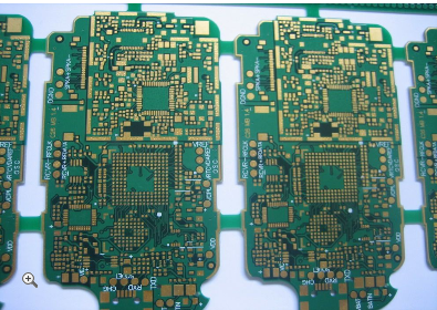
Enhancing Circuit Performance with Filter and Amplifier PCBs
In the rapidly advancing world of electronics, the demand for high-performance circuits has never been greater. Whether in telecommunications, medical devices, or consumer electronics, achieving optimal signal integrity and amplification is paramount. This is where the strategic integration of filter and amplifier printed circuit boards (PCBs) comes into play. These specialized PCBs are engineered to enhance circuit performance by minimizing noise, amplifying weak signals, and ensuring reliable operation across various frequencies. By delving into the design and application of these components, engineers and enthusiasts can unlock new levels of efficiency and functionality in their electronic systems.
Filters and amplifiers serve as the backbone of many modern electronic applications, from audio systems to radar technology. Filters, such as low-pass, high-pass, band-pass, and notch filters, are designed to allow specific frequency ranges to pass while attenuating others. This selectivity is crucial for reducing electromagnetic interference (EMI) and improving signal clarity. Amplifiers, on the other hand, boost the amplitude of signals, ensuring they are strong enough for subsequent processing or transmission. When combined on a well-designed PCB, these elements work synergistically to elevate overall circuit performance, making them indispensable in today's technology-driven landscape.
Design Considerations for Filter PCBs
Designing an effective filter PCB requires careful attention to component selection and layout. The choice of passive components, such as resistors, capacitors, and inductors, directly impacts the filter's frequency response and roll-off characteristics. For instance, in a low-pass filter, the values of these components determine the cutoff frequency, beyond which signals are attenuated. Additionally, the quality of these components—such as their tolerance and temperature stability—can affect the filter's performance under varying operating conditions. Engineers must also consider the PCB material, as substrates with low dielectric loss are preferred for high-frequency applications to minimize signal degradation.
Another critical aspect is the physical layout of the filter on the PCB. Proper grounding and shielding techniques are essential to prevent crosstalk and external interference. For example, placing filter components close to the signal source can reduce noise pickup along traces. Moreover, the use of ground planes and controlled impedance traces helps maintain signal integrity. In multi-layer PCBs, strategic layer stacking can isolate sensitive analog sections from noisy digital parts, further enhancing the filter's effectiveness. Simulation tools, such as SPICE models, are often employed to validate the design before fabrication, ensuring that the filter meets the desired specifications.
Amplifier PCB Implementation
Amplifiers are vital for boosting signal strength, but their performance heavily relies on PCB design. The selection of amplifier ICs or discrete transistors must align with the application's requirements, such as gain, bandwidth, and power consumption. For instance, operational amplifiers (op-amps) are commonly used for their versatility and high gain, but they require stable power supplies and proper biasing to avoid oscillations or distortion. The PCB layout must minimize parasitic capacitance and inductance, which can degrade high-frequency performance. This involves keeping input and output traces short and avoiding sharp bends that could introduce impedance mismatches.
Thermal management is another key consideration for amplifier PCBs, as power dissipation can lead to overheating and reduced reliability. Heat sinks, thermal vias, and adequate copper pours help dissipate heat efficiently. Additionally, decoupling capacitors placed near the amplifier's power pins suppress voltage fluctuations and noise, ensuring stable operation. For multi-stage amplifiers, isolation between stages prevents feedback and oscillation. Testing and characterization, such as measuring gain flatness and harmonic distortion, are crucial steps to verify that the amplifier performs as intended in the final PCB assembly.
Integration and Synergy
Combining filters and amplifiers on a single PCB requires a holistic approach to maximize synergy. For example, in a receiver circuit, a band-pass filter might precede an amplifier to eliminate out-of-band noise before amplification, thus improving the signal-to-noise ratio (SNR). The placement and routing of these components must be optimized to prevent interference; for instance, keeping the filter output trace short and direct to the amplifier input minimizes signal loss and pickup. This integration often involves trade-offs, such as balancing filter attenuation with amplifier gain to avoid over-amplification of noise or signal clipping.
Advanced techniques, such as using active filters that incorporate amplifiers within the filter design, can save space and enhance performance. These integrated solutions allow for tunable parameters, such as adjustable cutoff frequencies, through variable resistors or digital control. Furthermore, impedance matching between the filter and amplifier stages is critical to prevent reflections and ensure maximum power transfer. Simulation and prototyping play a vital role in refining these designs, allowing engineers to iterate and optimize for specific applications, from audio processing to RF communications.
Applications and Future Trends
The applications of filter and amplifier PCBs are vast and growing. In wireless communication systems, they are used in transceivers to enhance signal quality and range. Medical devices, such as ECG monitors, rely on them to amplify bio-signals while filtering out interference from other equipment. Automotive electronics employ these PCBs in infotainment and radar systems, where reliability and performance are critical. As Internet of Things (IoT) devices proliferate, the demand for compact, low-power filter and amplifier solutions will continue to rise, driving innovations in PCB technology.
Looking ahead, trends like 5G, artificial intelligence, and autonomous vehicles will push the boundaries of filter and amplifier PCB design. Higher frequency bands will require materials with better dielectric properties, while miniaturization will emphasize embedded components and multi-chip modules. Additionally, the integration of digital signal processing (DSP) with analog filters and amplifiers will enable adaptive systems that can dynamically adjust to changing conditions. By staying abreast of these developments, engineers can continue to enhance circuit performance, paving the way for next-generation electronic innovations.
REPORT


