-
 Agriculture
-
 Health-Care
-
 Environment
-
 Construction-Real-Estate
-
 Tools-Hardware
-
 Home-Garden
-
 Furniture
-
 Luggage-Bags-Cases
-
 Medical-devices-Supplies
-
 Gifts-Crafts
-
 Sports-Entertainment
-
 Food-Beverage
-
 Vehicles-Transportation
-
 Power-Transmission
-
 Material-Handling
-
 Renewable-Energy
-
 Safety
-
 Testing-Instrument-Equipment
-
 Construction-Building-Machinery
-
 Pet-Supplies
-
 Personal-Care-Household-Cleaning
-
 Vehicle-Accessories-Electronics-Tools
-
 School-Office-Supplies
-
 Packaging-Printing
-
 Mother-Kids-Toys
-
 Business-Services
-
 Commercial-Equipment-Machinery
-
 Apparel-Accessories
-
 Security
-
 Shoes-Accessories
-
 Vehicle-Parts-Accessories
-
 Jewelry-Eyewear-Watches-Accessories
-
 Lights-Lighting
-
 Fabric-Textile-Raw-Material
-
 Fabrication-Services
-
 Industrial-Machinery
-
 Consumer-Electronics
-
 Electrical-Equipment-Supplies
-
 Electronic-Components-Accessories-Telecommunications
-
 Home-Appliances
-
 Beauty
-
 Chemicals
-
 Rubber-Plastics
-
 Metals-Alloys
- Masonry Materials
- Curtain Walls & Accessories
- Earthwork Products
- Fireproofing Materials
- Heat Insulation Materials
- Plastic Building Materials
- Building Boards
- Soundproofing Materials
- Timber
- Waterproofing Materials
- Balustrades & Handrails
- Bathroom & Kitchen
- Flooring & Accessories
- Tiles & Accessories
- Door, Window & Accessories
- Fireplaces & Stoves
- Floor Heating Systems & Parts
- Stairs & Stair Parts
- Ceilings
- Elevators & Escalators
- Stone
- Countertops, Vanity Tops & Table Tops
- Mosaics
- Metal Building Materials
- Multifunctional Materials
- Ladders & Scaffoldings
- Mouldings
- Corner Guards
- Decorative Films
- Formwork
- Building & Industrial Glass
- Other Construction & Real Estate
- Wallpapers/Wall panels
- HVAC System & Parts
- Outdoor Facilities
- Prefabricated Buildings
- Festive & Party Supplies
- Bathroom Products
- Household Sundries
- Rain Gear
- Garden Supplies
- Household Cleaning Tools & Accessories
- Lighters & Smoking Accessories
- Home Storage & Organization
- Household Scales
- Smart Home Improvement
- Home Textiles
- Kitchenware
- Drinkware & Accessories
- Dinnerware, Coffee & Wine
- Home Decor
- Golf
- Fitness & Body Building
- Amusement Park Facilities
- Billiards, Board Game,Coin Operated Games
- Musical Instruments
- Outdoor Affordable Luxury Sports
- Camping & Hiking
- Fishing
- Sports Safety&Rehabilitation
- Ball Sports Equipments
- Water Sports
- Winter Sports
- Luxury Travel Equipments
- Sports Shoes, Bags & Accessories
- Cycling
- Other Sports & Entertainment Products
- Artificial Grass&Sports Flooring&Sports Court Equipment
- Scooters
- Food Ingredients
- Honey & Honey Products
- Snacks
- Nuts & Kernels
- Seafood
- Plant & Animal Oil
- Beverages
- Fruit & Vegetable Products
- Frog & Escargot
- Bean Products
- Egg Products
- Dairy Products
- Seasonings & Condiments
- Canned Food
- Instant Food
- Baked Goods
- Other Food & Beverage
- Meat & Poultry
- Confectionery
- Grain Products
- Feminie Care
- Hair Care & Styling
- Body Care
- Hands & Feet Care
- Hygiene Products
- Men's Grooming
- Laundry Cleaning Supplies
- Travel Size & Gift Sets
- Room Deodorizers
- Other Personal Care Products
- Pest Control Products
- Special Household Cleaning
- Floor Cleaning
- Kitchen & Bathroom Cleaning
- Oral Care
- Bath Supplies
- Yellow Pages
- Correction Supplies
- Office Binding Supplies
- Office Cutting Supplies
- Board Erasers
- Office Adhesives & Tapes
- Education Supplies
- Pencil Cases & Bags
- Notebooks & Writing Pads
- File Folder Accessories
- Calendars
- Writing Accessories
- Commercial Office Supplies
- Pencil Sharpeners
- Pens
- Letter Pad/Paper
- Paper Envelopes
- Desk Organizers
- Pencils
- Markers & Highlighters
- Filing Products
- Art Supplies
- Easels
- Badge Holder & Accessories
- Office Paper
- Printer Supplies
- Book Covers
- Other Office & School Supplies
- Stationery Set
- Boards
- Clipboards
- Stamps
- Drafting Supplies
- Stencils
- Electronic Dictionary
- Books
- Map
- Magazines
- Calculators
- Baby & Toddler Toys
- Educational Toys
- Classic Toys
- Dress Up & Pretend Play
- Toy Vehicle
- Stuffed Animals & Plush Toys
- Outdoor Toys & Structures
- Balloons & Accessories
- Baby Food
- Children's Clothing
- Baby Supplies & Products
- Maternity Clothes
- Kids Shoes
- Baby Care
- Novelty & Gag Toys
- Dolls & Accessories
- Puzzle & Games
- Blocks & Model Building Toys
- Toddler Clothing
- Baby Clothing
- Kids' Luggage & Bags
- Arts, Crafts & DIY Toys
- Action & Toy Figures
- Baby Appliances
- Hobbies & Models
- Remote Control Toys
- Promotional Toys
- Pregnancy & Maternity
- Hygiene Products
- Kid's Textile&Bedding
- Novelty & Special Use
- Toy Weapons
- Baby Gifts
- Baby Storage & Organization
- Auto Drive Systems
- ATV/UTV Parts & Accessories
- Marine Parts & Accessories
- Other Auto Parts
- Trailer Parts & Accessories
- Auto Transmission Systems
- Train Parts & Accessories
- Universal Parts
- Railway Parts & Accessories
- Auto Brake Systems
- Aviation Parts & Accessories
- Truck Parts & Accessories
- Auto Suspension Systems
- Auto Lighting Systems
- New Energy Vehicle Parts & Accessories
- Auto Steering Systems
- Wheels, Tires & Accessories
- Bus Parts & Accessories
- Auto Performance Parts
- Cooling System
- Go-Kart & Kart Racer Parts & Accessories
- Air Conditioning Systems
- Heavy Duty Vehicle Parts & Accessories
- Auto Electrical Systems
- Auto Body Systems
- Auto Engine Systems
- Container Parts & Accessories
- Motorcycle Parts & Accessories
- Refrigeration & Heat Exchange Equipment
- Machine Tool Equipment
- Food & Beverage Machinery
- Agricultural Machinery & Equipment
- Apparel & Textile Machinery
- Chemical Machinery
- Packaging Machines
- Paper Production Machinery
- Plastic & Rubber Processing Machinery
- Industrial Robots
- Electronic Products Machinery
- Metal & Metallurgy Machinery
- Woodworking Machinery
- Home Product Manufacturing Machinery
- Machinery Accessories
- Environmental Machinery
- Machinery Service
- Electrical Equipment Manufacturing Machinery
- Industrial Compressors & Parts
- Tobacco & Cigarette Machinery
- Production Line
- Used Industrial Machinery
- Electronics Production Machinery
- Other Machinery & Industrial Equipment
- Camera, Photo & Accessories
- Portable Audio, Video & Accessories
- Television, Home Audio, Video & Accessories
- Video Games & Accessories
- Mobile Phone & Accessories
- Electronic Publications
- Earphone & Headphone & Accessories
- Speakers & Accessories
- Smart Electronics
- TV Receivers & Accessories
- Mobile Phone & Computer Repair Parts
- Chargers, Batteries & Power Supplies
- Used Electronics
- VR, AR, MR Hardware & Software
- Projectors & Presentation Equipments
- Other Consumer Electronics
- Cables & Commonly Used Accessories
- Computer Hardware & Software
- Displays, Signage and Optoelectronics
- Discrete Semiconductors
- Wireless & IoT Module and Products
- Telecommunications
- Connectors, Terminals & Accessories
- Development Boards, Electronic Modules and Kits
- Circuit Protection
- Sensors
- Isolators
- Audio Components and Products
- Integrated Circuits
- Power Supplies
- Relays
- RF, Microwave and RFID
- Electronic Accessories & Supplies
- Passive Components
- PCB & PCBA
- Air Quality Appliances
- Home Appliance Parts
- Heating & Cooling Appliances
- Small Kitchen Appliances
- Laundry Appliances
- Water Heaters
- Water Treatment Appliances
- Refrigerators & Freezers
- Personal Care & Beauty Appliances
- Major Kitchen Appliances
- Cleaning Appliances
- Second-hand Appliances
- Smart Home Appliances
- Other Home Appliances
- Energy Chemicals
- Inorganic Chemicals
- Basic Organic Chemicals
- Agrochemicals
- Admixture & Additives
- Catalysts & Chemical Auxiliary Agents
- Pigments & Dyestuff
- Coating & Paint
- Daily Chemicals
- Polymer
- Organic Intermediate
- Adhesives & Sealants
- Chemical Waste
- Biological Chemical Products
- Surface Treatment Chemicals
- Painting & Coating
- Chemical Reagents
- Flavor & Fragrance
- Non-Explosive Demolition Agents
- Other Chemicals
- Custom Chemical Services
Wireless & IoT Module and Products
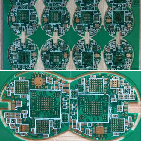
High Precision Circuit Board PCB Deep Hole Technology for Industry 40 Standards
In the era of Industry 4.0, the demand for high-precision electronic components has surged, driven by the need for smarter, faster, and more reliable devices. At the heart of this technological revolution lies the High Precision Circuit Board (PCB) Deep Hole Technology, a critical enabler for advanced manufacturing standards. This technology ensures that PCBs meet the stringent requirements of modern applications, such as 5G communications, automotive electronics, and IoT devices. By achieving unparalleled accuracy in drilling microvias and deep holes, this innovation paves the way for higher density interconnects and improved performance. But what exactly makes this technology so vital, and how does it align with Industry 4.0 standards? Let’s delve deeper.
The Role of Deep Hole Technology in High-Precision PCBs
Deep hole technology in PCBs refers to the process of creating microvias and through-holes with exceptional precision, often with diameters as small as a few micrometers. These holes are essential for establishing electrical connections between multiple layers of a PCB, enabling complex circuitry in compact designs. As devices become smaller and more powerful, the need for deeper and narrower holes has grown exponentially.
Traditional drilling methods often fall short in meeting these demands due to limitations in accuracy and repeatability. High-precision deep hole technology, however, leverages advanced laser drilling and mechanical techniques to achieve consistent results. This ensures that even the most intricate designs can be realized without compromising on reliability or performance.
Alignment with Industry 4.0 Standards
Industry 4.0 emphasizes automation, data exchange, and smart manufacturing, all of which require PCBs to be more robust and precise. High-precision deep hole technology aligns perfectly with these standards by enabling the production of PCBs that can withstand harsh environments and deliver consistent performance. For instance, in automotive electronics, where temperature fluctuations and vibrations are common, deep hole technology ensures durable interconnects that resist failure.
Moreover, this technology supports the integration of sensors and IoT modules, which are central to Industry 4.0. By facilitating higher component density and better signal integrity, deep hole technology helps create PCBs that are not only smaller but also smarter. This is crucial for applications like predictive maintenance and real-time monitoring, where reliability is paramount.
Advanced Techniques in Deep Hole Drilling
One of the key advancements in deep hole technology is the use of ultrafast lasers, such as picosecond and femtosecond lasers. These lasers minimize thermal damage to the surrounding material, ensuring clean and precise holes. This is particularly important for high-frequency applications, where even minor imperfections can degrade signal quality.
Another technique involves the use of automated optical inspection (AOI) systems to verify hole quality in real-time. These systems detect defects like misalignment or incomplete drilling, allowing for immediate corrections. Such automation not only improves yield but also reduces waste, aligning with the sustainability goals of Industry 4.0.
Challenges and Future Prospects
Despite its advantages, high-precision deep hole technology faces challenges such as high equipment costs and the need for skilled operators. The initial investment in laser drilling systems and AOI tools can be significant, making it difficult for smaller manufacturers to adopt this technology. However, as the demand for high-performance PCBs grows, economies of scale are expected to drive down costs.
Looking ahead, researchers are exploring new materials and techniques to further enhance deep hole technology. For example, the use of hybrid drilling methods, combining mechanical and laser drilling, could offer even greater precision and efficiency. Additionally, advancements in AI and machine learning may enable smarter inspection systems, further reducing defects and improving productivity.
Conclusion
High Precision Circuit Board PCB Deep Hole Technology is a cornerstone of modern electronics manufacturing, enabling the creation of devices that meet the rigorous demands of Industry 4.0. From its role in enabling high-density interconnects to its alignment with smart manufacturing standards, this technology is indispensable for the future of electronics. As innovations continue to emerge, the potential for even greater precision and efficiency promises to unlock new possibilities across industries.

Ensuring Superior Quality with High Precision Circuit Board Deep Hole Control
In the rapidly evolving world of electronics, the demand for high-performance circuit boards has never been greater. One of the critical factors in achieving superior quality lies in the precision control of deep holes in circuit boards. These deep holes, often referred to as microvias or through-holes, play a pivotal role in ensuring the reliability and functionality of modern electronic devices. As technology advances, the need for smaller, more intricate circuit boards with higher density interconnects has made deep hole control a cornerstone of manufacturing excellence. This article delves into the intricacies of ensuring superior quality through high-precision deep hole control, exploring its significance, challenges, and innovative solutions.
The Importance of Deep Hole Precision in Circuit Boards
Deep holes in circuit boards are essential for creating electrical connections between different layers of the board. These holes must be drilled with extreme precision to ensure proper alignment and conductivity. Even the slightest deviation can lead to signal loss, short circuits, or complete board failure. High-precision deep hole control is particularly crucial in applications such as aerospace, medical devices, and telecommunications, where reliability is non-negotiable.
Moreover, as electronic devices become more compact, the size of these holes continues to shrink. This trend places additional demands on manufacturing processes, requiring advanced drilling techniques and equipment. The ability to maintain consistent hole diameter, depth, and wall smoothness is vital for achieving the desired electrical performance and longevity of the circuit board.
Advanced Drilling Technologies for High Precision
To meet the stringent requirements of modern circuit boards, manufacturers are turning to advanced drilling technologies. Laser drilling, for instance, has emerged as a preferred method for creating microvias with diameters as small as a few micrometers. Unlike mechanical drilling, laser drilling offers unparalleled precision and minimizes the risk of material deformation or damage.
Another innovative approach is the use of computer numerical control (CNC) machines equipped with high-speed spindles. These machines can achieve exceptional accuracy and repeatability, ensuring that each hole is drilled to exact specifications. Additionally, real-time monitoring systems can detect and correct deviations during the drilling process, further enhancing quality control.
Material Considerations for Optimal Deep Hole Quality
The choice of materials plays a significant role in the quality of deep holes in circuit boards. For instance, the substrate material must have excellent thermal and mechanical properties to withstand the drilling process without warping or delaminating. High-performance materials like polyimide and PTFE are often used in demanding applications due to their stability and durability.
Furthermore, the quality of the conductive plating inside the holes is equally important. Electroless copper plating and other advanced metallization techniques ensure uniform coverage and strong adhesion, preventing voids or cracks that could compromise electrical connectivity. Proper material selection and processing are critical to achieving reliable and high-quality deep holes.
Quality Assurance and Testing Methods
Ensuring the quality of deep holes requires rigorous testing and inspection protocols. Automated optical inspection (AOI) systems are commonly used to verify hole dimensions, placement accuracy, and surface finish. These systems can detect defects such as misalignment, incomplete drilling, or plating inconsistencies with high precision.
In addition to visual inspections, electrical testing methods like continuity testing and impedance measurement are employed to validate the functional integrity of the holes. Cross-sectional analysis may also be performed to examine the internal structure of the holes and identify any hidden defects. By combining multiple testing approaches, manufacturers can guarantee the highest standards of quality and reliability.
Future Trends in Deep Hole Control
The future of deep hole control in circuit boards is poised for exciting advancements. With the rise of 5G technology, Internet of Things (IoT) devices, and artificial intelligence, the demand for ultra-high-density interconnects will continue to grow. This will drive the development of even more precise drilling techniques and materials capable of meeting these challenges.
Emerging technologies such as additive manufacturing (3D printing) and nanotechnology may also revolutionize the way deep holes are created and controlled. These innovations promise to deliver unprecedented levels of precision and customization, opening new possibilities for circuit board design and performance. As the industry evolves, staying at the forefront of these developments will be key to maintaining a competitive edge.

Optimizing Deep Hole Accuracy in High Precision Circuit Board PCB Manufacturing
In the rapidly evolving world of electronics, high precision circuit board (PCB) manufacturing plays a pivotal role in ensuring the performance and reliability of modern devices. One of the most critical challenges in this field is optimizing deep hole accuracy, as even the slightest deviation can lead to significant functional issues. Deep holes, often used for vias and through-holes, must meet stringent tolerances to ensure proper electrical connectivity and mechanical stability. This article delves into the intricacies of optimizing deep hole accuracy, exploring advanced techniques, materials, and technologies that are reshaping the PCB manufacturing landscape.
The Importance of Deep Hole Accuracy in PCB Manufacturing
Deep hole accuracy is paramount in high precision PCB manufacturing because it directly impacts the board's electrical performance and structural integrity. In multi-layer PCBs, deep holes serve as conduits for electrical signals between layers, and any misalignment or inconsistency can lead to signal loss, cross-talk, or even complete circuit failure. Moreover, as PCBs become increasingly miniaturized, the demand for smaller and deeper holes with tighter tolerances has grown exponentially.
Beyond electrical performance, deep hole accuracy also affects the mechanical robustness of the PCB. Poorly drilled holes can weaken the board, making it susceptible to cracking or delamination during assembly or operation. This is particularly critical in applications such as aerospace, medical devices, and automotive electronics, where reliability is non-negotiable. Thus, optimizing deep hole accuracy is not just a technical challenge but a necessity for achieving high-quality PCB manufacturing.
Advanced Drilling Techniques for Precision Deep Holes
Traditional mechanical drilling methods, while effective for standard applications, often fall short when it comes to high precision deep holes. To address this, manufacturers are turning to advanced techniques such as laser drilling and controlled-depth drilling. Laser drilling, for instance, offers unparalleled precision by using focused laser beams to create holes with diameters as small as a few micrometers. This method is especially useful for microvias and high-density interconnect (HDI) PCBs.
Another promising approach is controlled-depth drilling, which combines mechanical drilling with real-time monitoring systems to ensure consistent hole depth. By integrating sensors and feedback mechanisms, manufacturers can adjust drilling parameters on the fly, minimizing deviations and improving accuracy. These advanced techniques not only enhance precision but also reduce the risk of tool wear and material damage, leading to higher yields and lower production costs.
Material Considerations for Optimal Deep Hole Quality
The choice of materials significantly influences deep hole accuracy in PCB manufacturing. For instance, the substrate material must exhibit excellent thermal and mechanical properties to withstand the drilling process without deforming or delaminating. High-performance materials like polyimide and PTFE are often preferred for their stability and low thermal expansion coefficients.
Additionally, the quality of the copper plating inside the holes plays a crucial role in ensuring electrical conductivity and mechanical strength. Electroless copper plating and direct metallization techniques are commonly used to achieve uniform plating thickness, even in deep holes. By selecting the right materials and plating methods, manufacturers can enhance hole quality and reliability, meeting the stringent demands of modern electronics.
The Role of Automation and AI in Deep Hole Optimization
Automation and artificial intelligence (AI) are revolutionizing PCB manufacturing by enabling real-time monitoring and adaptive control of drilling processes. Automated drilling systems equipped with AI algorithms can analyze vast amounts of data to identify patterns and predict potential issues before they occur. This proactive approach minimizes errors and ensures consistent hole quality across large production runs.
Furthermore, machine learning models can optimize drilling parameters such as speed, feed rate, and spindle rotation based on material properties and hole specifications. By continuously learning from past operations, these systems can fine-tune their performance, achieving unprecedented levels of accuracy and efficiency. The integration of automation and AI not only enhances deep hole accuracy but also reduces production time and waste, making it a game-changer for high precision PCB manufacturing.
Quality Control and Testing for Deep Hole Accuracy
Ensuring deep hole accuracy requires rigorous quality control and testing protocols. Non-destructive testing methods like X-ray inspection and automated optical inspection (AOI) are widely used to verify hole dimensions, alignment, and plating quality. X-ray imaging, in particular, allows manufacturers to inspect internal features without damaging the PCB, making it ideal for high precision applications.
In addition to advanced imaging techniques, electrical testing is employed to assess the conductivity and integrity of the holes. Flying probe testers and boundary scan testing can detect open circuits, short circuits, and other defects that may compromise performance. By combining these testing methods, manufacturers can identify and rectify issues early in the production process, ensuring that only flawless PCBs reach the end user.
In conclusion, optimizing deep hole accuracy in high precision PCB manufacturing is a multifaceted challenge that demands cutting-edge techniques, materials, and technologies. From advanced drilling methods to AI-driven automation and rigorous quality control, every aspect plays a vital role in achieving the desired precision and reliability. As the electronics industry continues to push the boundaries of miniaturization and performance, the importance of deep hole accuracy will only grow, driving further innovation in this critical field.
REPORT

